尋找感興趣的產品?
Electronic Design Automation
Discover the next generation of electronic design automation software
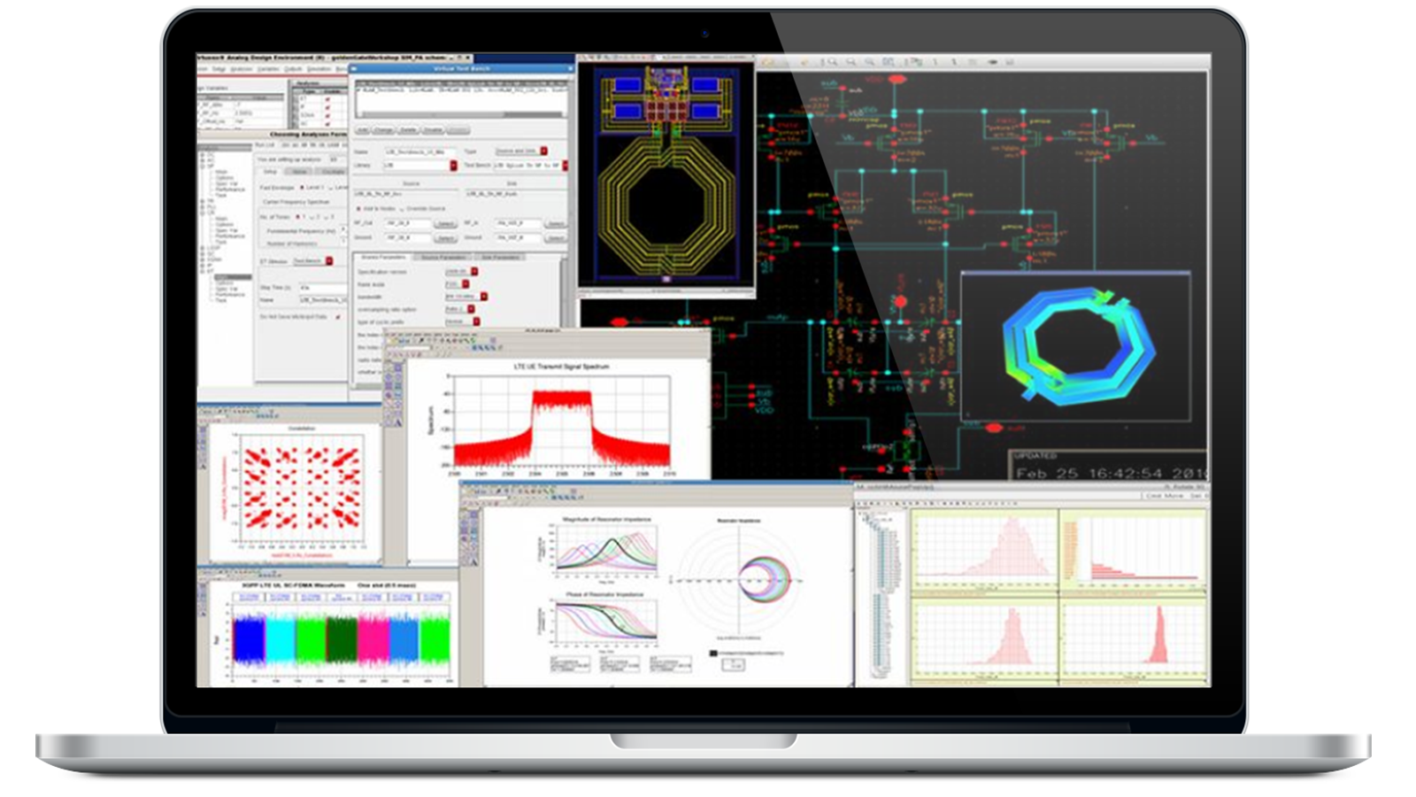
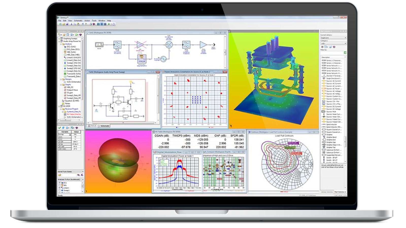
Model, Simulate, and Optimize with EDA Software
Shorten design cycles to achieve first-pass design success. Our next-generation integrated electronic design automation (EDA) software provides engineers with tools that simplify multi-domain insights for RF and microwave, 5G / 6G, and high-speed digital printed circuit boards (PCB) throughout the design cycle.
With partnerships spanning RFIC and MMIC foundries, Keysight offers accurate models and a broad range of validated Process Design Kits (PDKs) to ensure a streamlined workflow from schematic capture to design rule checking (DRC). Additionally, Keysight collaborates with leading component manufacturers to provide an extensive parts library, accelerating the design process. Keysight EDA accelerates design confidence from simulation to verification and compliance with built-in design templates, extensive component libraries, robust modeling, and precise simulations addressing complex electronic design challenges with precision and efficiency.
Start Your Next Design with Keysight EDA Tools
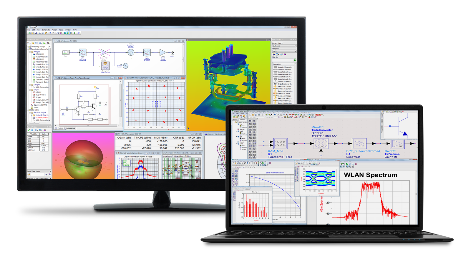
The Keysight suite of EDA tools seamlessly integrates device modeling, circuit design, EM simulation, layout capabilities, and system-level modeling. Keysight’s open solutions approach for workflow enablement ensures that our EDA software interoperates with other EDA software from our ecosystem partners. Combine process design kits (PDKs) with our circuit simulators to increase your confidence in achieving design success.
Explore Keysight EDA Software Suites


EDA Software in Your Design Workflow
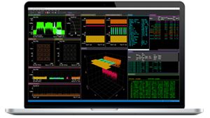
Circuit Design and Simulation
EDA software for circuit design and simulation accelerates product development by reducing the time engineers spend in the design and simulation phases. Its libraries and customized simulators reduce setup time. The software seamlessly integrates circuit design, EM simulation, layout capabilities, and system-level modeling, reducing time spent importing and exporting designs and fixing errors associated with changing tools. Improvements in data analytics enable faster analysis and design decisions.


Physical Design and Simulation
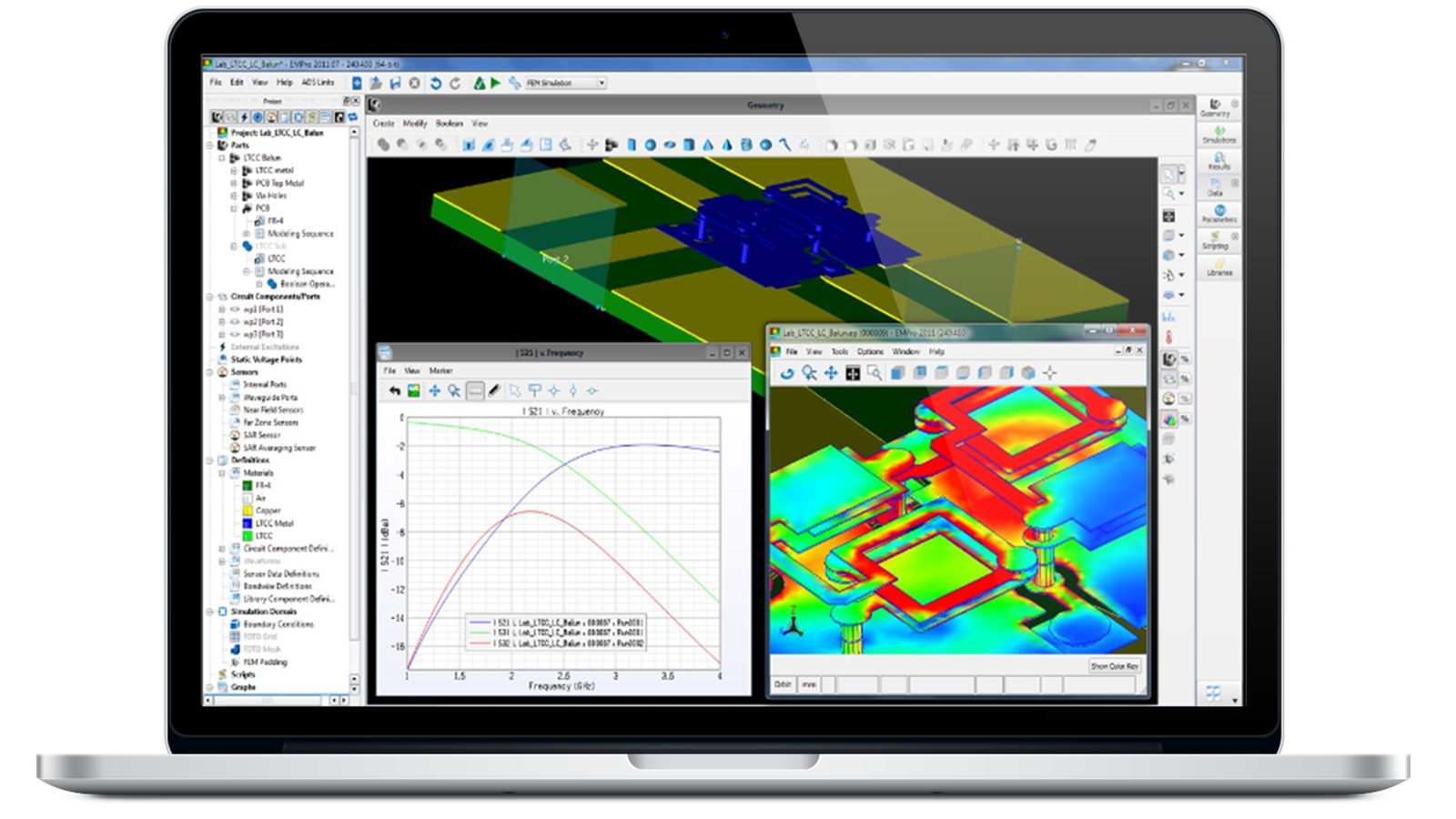
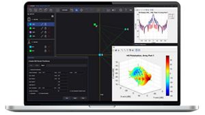
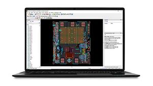
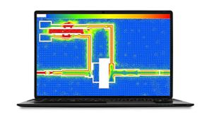
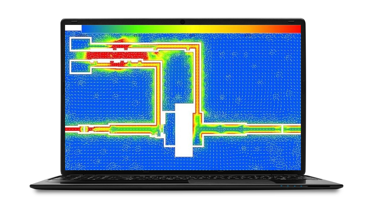
EDA tools for EM simulation enable designers to accurately model large portions of the system and the entire system. Additionally, integrating 3D EM modeling with traditional circuit simulation is one method to radically simplify your design flow. Keysight ADS offers a parameterized 3D component design kit that enables designers to quickly draw, codesign, and optimize 3D components with other schematic components.


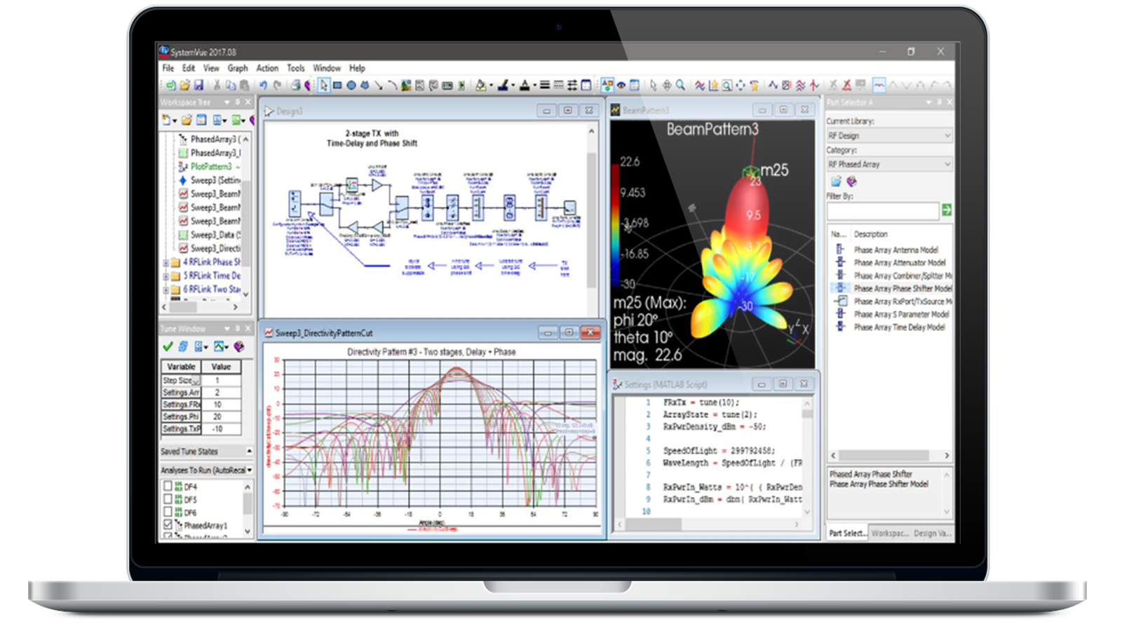
System Design and Simulation
EDA software for RF system design combines multi-domain modeling with simulation for complex RF systems in one collaborative design environment. Going beyond math-based modeling with a complete design workflow optimized for RF, Keysight System Design brings decades of industry leadership in RF measurement science into your modeling environment.


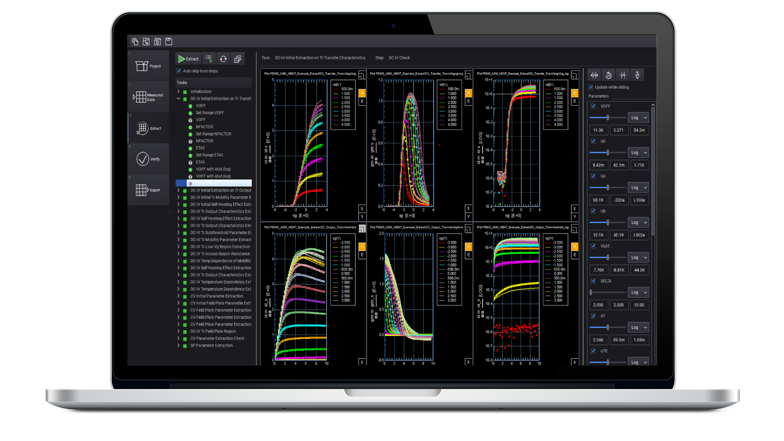
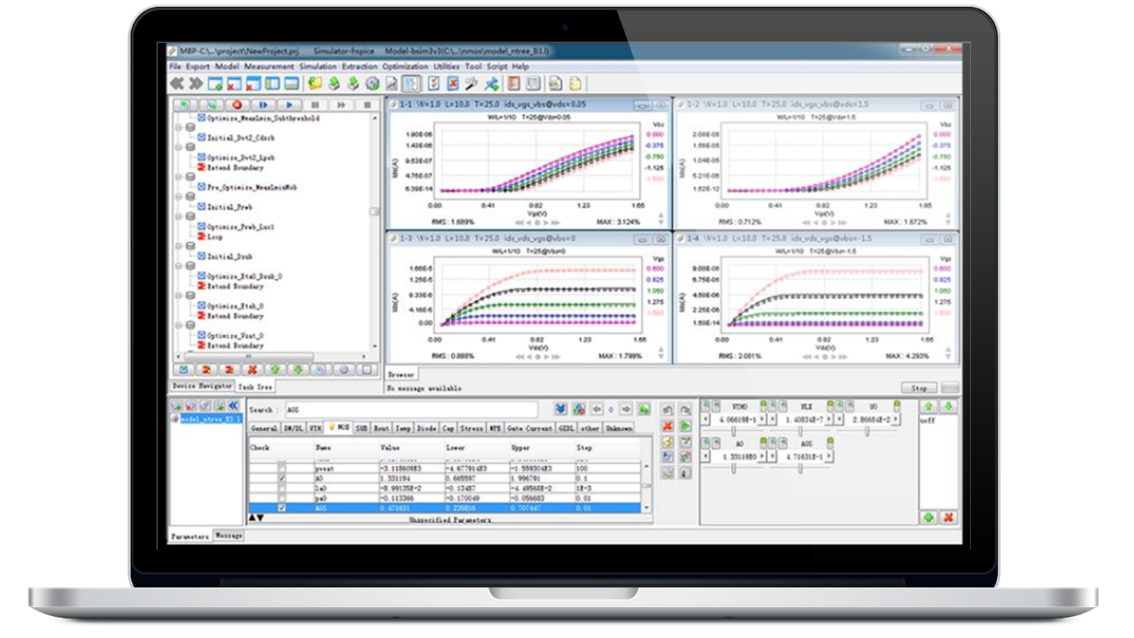
Device Modeling and Characterization
EDA tools enable the characterization and modeling of cutting-edge CMOS and compound semiconductor devices. Keysight is the only vendor that provides end-to-end modeling solutions from automated measurements, device model extraction, and qualification to final PDK validation. Comprehensive modeling services are available with support from Keysight experts and advanced labs.


Engineering Data Management
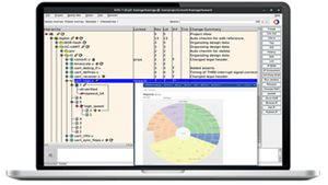
Empower local or multi-site design teams to collaborate efficiently on all types of complex hardware designs — analog, digital, RF, and mixed-signal. Elevate design reuse and manage the process of IP creation and publication for internal and third-party IP with multiple levels of built-in security and customizable workflows. Define, manage, and execute a simulation or test process and manage the big data produced by these processes.


Simulate Five Times Faster by Moving Simulation to the Cloud
The latest innovations in cloud technology have advanced to the world of electronic design and simulation. Design workspaces can be gigabytes in size, but the simulation files you need may only be 10’s of megabytes. You don’t need to utilize the entire workspace file to simulate.
With cloud simulation, the software only sends the files that it needs in order to run the simulation. Using high-performance computing and cloud simulation, design teams are cutting their simulation times by over 80%.
Read Our Reviews
“In choosing design tools, we needed to consider the whole flow, from the schematic to the 3D simulations. Our engineers need to be familiar with the tools, and that is one of the reasons why we chose Keysight’s PathWave ADS as the core tool.”
Dr. Xu Xhu
Director of Technology
Menlo Micro
Read Our Reviews
“We have a way to collect a huge amount of S-parameter data which helps us to select the golden die of the AC performance. It is very helpful to have a very accurate SPICE model for high-speed circuit design.”
Dr. Sadayuki Yoshitomi
Kioxia Corporation
Read Our Reviews
“I used GoldenGate day-in and day-out for all of my W-band mmWave circuit and system-level simulations to do system-level linearity, noise figure, and other characterizations across the frequency ranges.”
Amit Singh
Technical Staff
Nokia Bell Labs
Read Our Reviews
“The data points are bang-on thermal simulations, and the reliability looks good, with a very benign PA power degradation over time. These were not given before we started our virtual thermal analysis.”
Alan Wong
Sr. Vice President of Engineering
EnSilica
Read Our Reviews
“A full-up workspace in PathWave System Design with our Sys-Parameters models speeds everything up. It's a step beyond anything we've seen out there for RF system reference designs.”
David Brown
Systems Integration Engineer
Analog Devices
Read Our Reviews
“When we’re very careful with our design and do a full modeling work up on an amplifier in PathWave ADS, spending extra time on different transistor models, we can get through with one variant.”
Doug Jorgesen
VP of Systems and Applications
at Marki Microwave
Read Our Reviews
“The Keysight people’s knowledge and skills with PathWave ADS help us catch more issues earlier and work through situations like scripting, integration, and more that are extremely valuable in our mmWave RF component design efforts.”
Dr. Sayed Tabatabaei
Founder and CEO,
mmTron
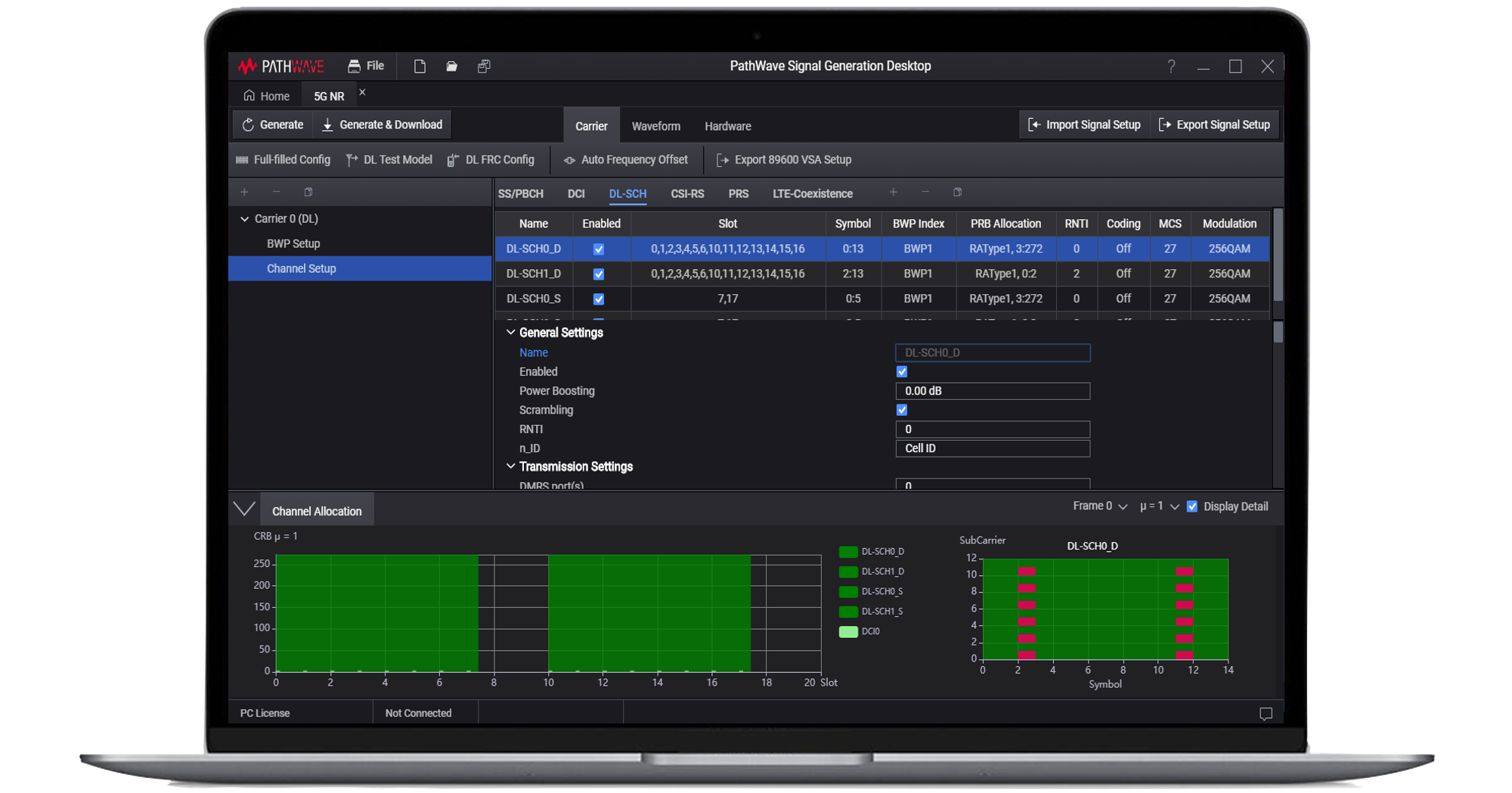
Foundry Process Design Kits
Integrated circuit (IC) foundries offer semiconductor processes that use PDKs containing active and passive device simulation models for IC design. Keysight EDA tools work closely with foundries to offer high-frequency PDKs in Si, SiGe, GaAs, InP, and GaN processes.
When choosing a foundry PDK, you must be sure that the models meet foundry manufacturing requirements. Foundries validate and distribute all PDKs provided for Keysight simulators, guaranteeing that the models behave optimally for first-pass design success.

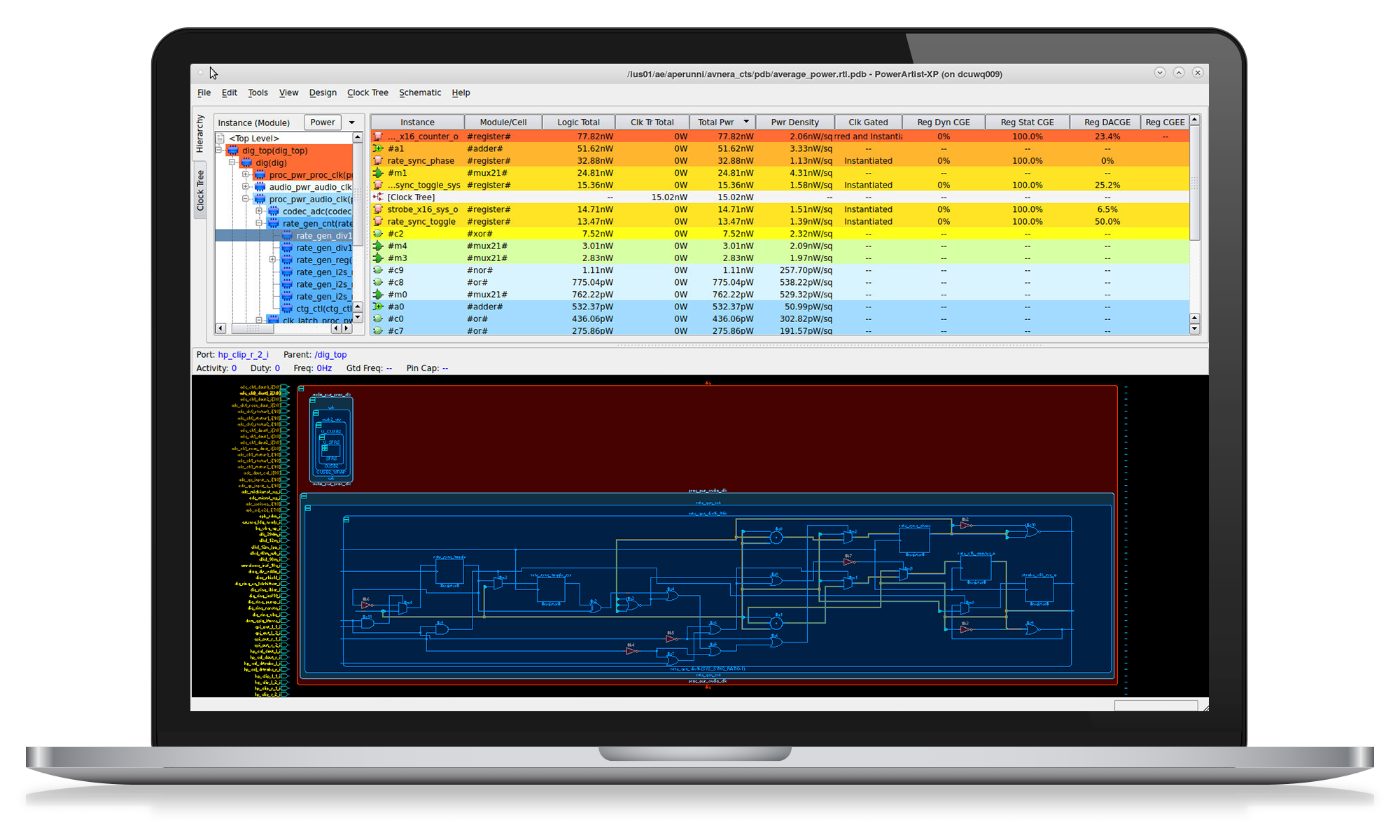
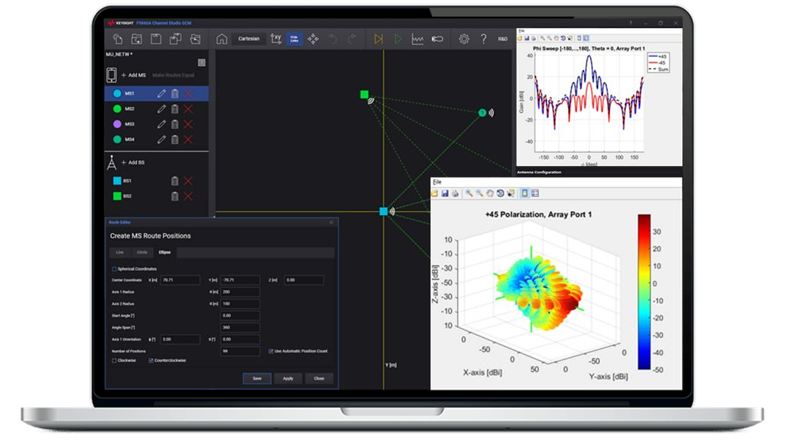
_13926v2.png)
_13926v2.png "EDA tools for circuit design, RF modeling, and antenna design")
Keysight EDA Software: 40 Years of Design Success
Explore our history of technical innovation, customer support, training, and industry leadership across the markets we serve in EDA software.
Protect Your Innovation Investment


Related Use Cases

How to Design Soft-Switching Power Converters

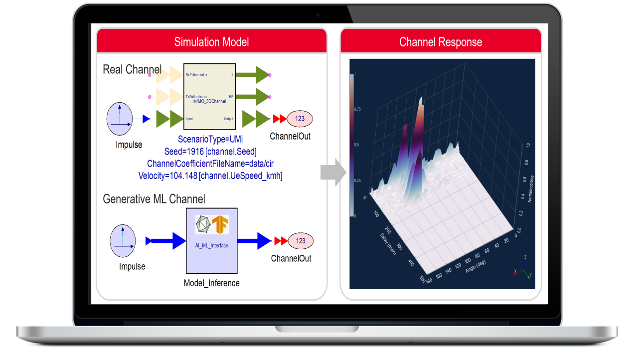
How to Simulate AI-Driven Air Interface PHY for 6G Research
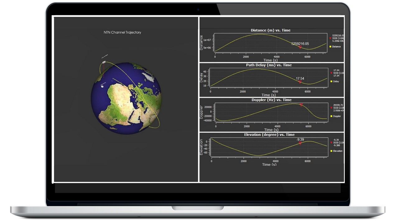
How to Simulate 5G NTN Transmission Paths
How to Simulate an RF Circuit

How to Design Robust 5G Power Amplifiers for the Real World
How to Design A Stable RF Power Amplifier

How to Simulate Digital Pre-Distortion For Power Amplifier Design
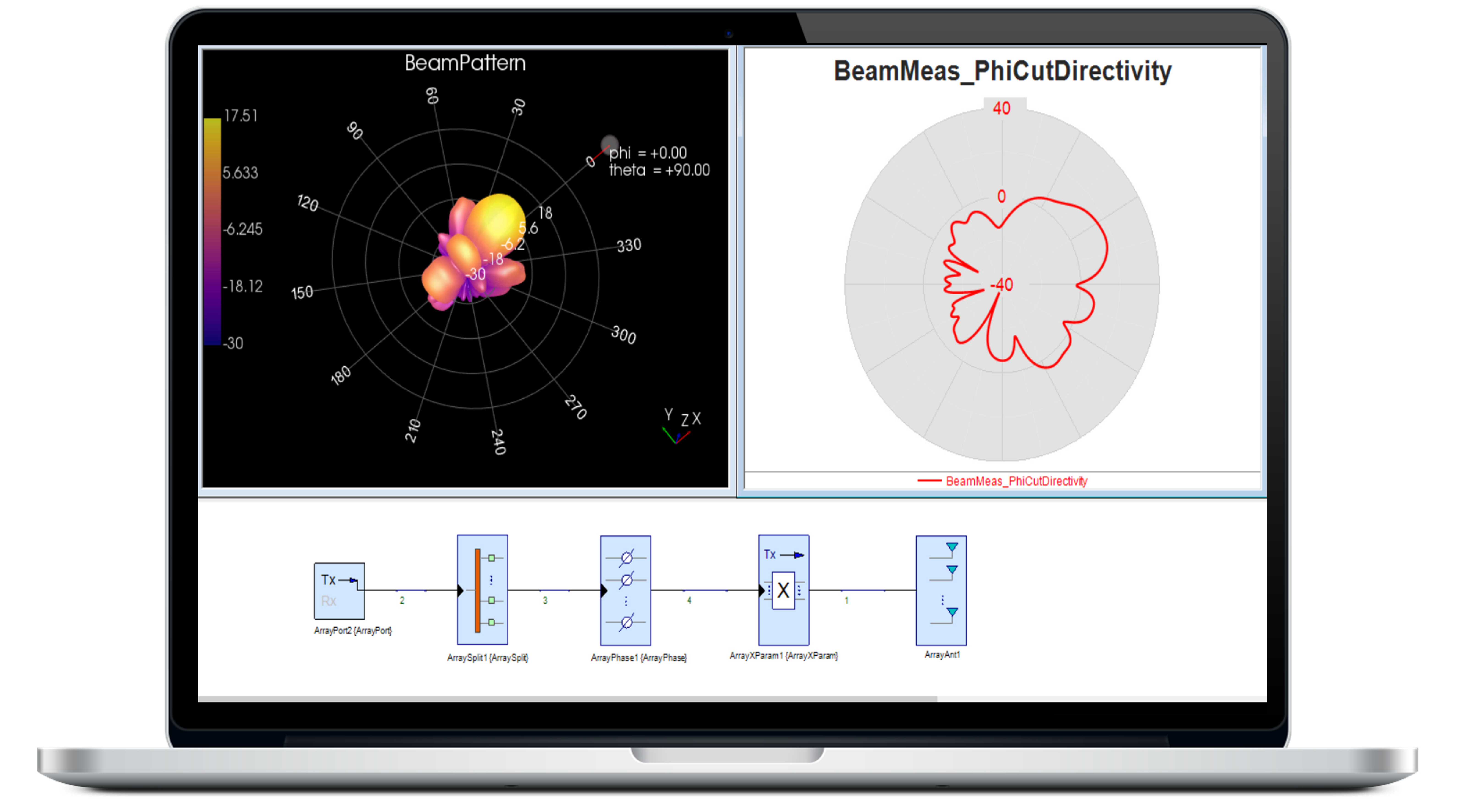
How to Capture Load Pull Effects on Beamforming


How to Design Multi-Technology mmWave Phased Arrays
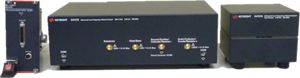
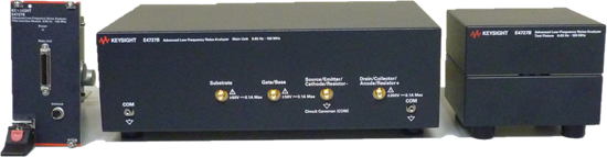
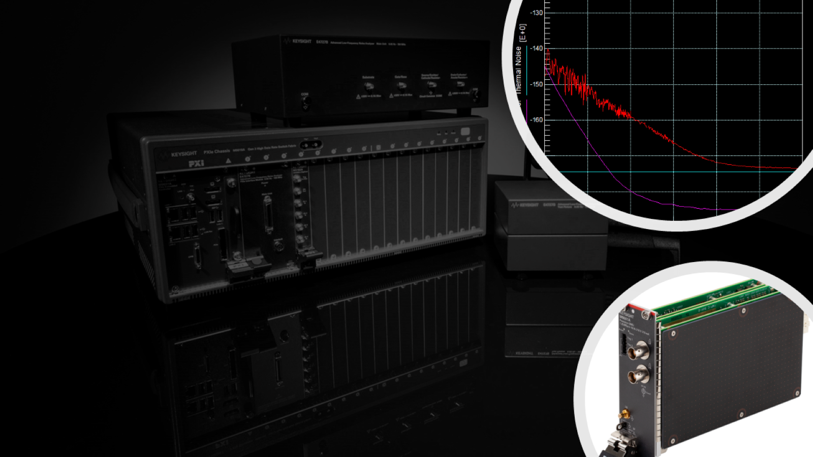
How to Measure Low-Frequency Noise Accurately
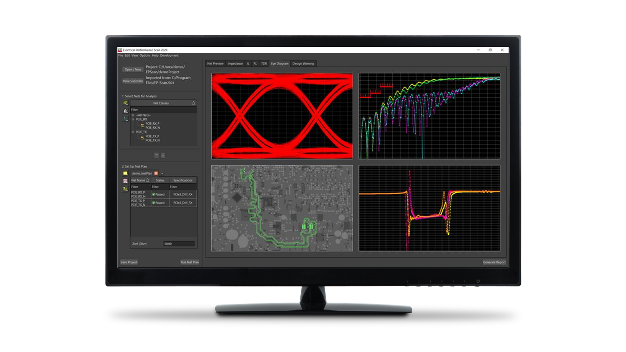
How to Determine DDR5 Controlled Trace Impedance
How to Analyze Signal Integrity using Layout Geometry
Learn More About EDA Software


EDA
Software and Tools – FAQ
Electronic design automation (EDA) is a Computer-Aided Design (CAD) category of software tools for designing electronic circuits and systems. The tools work together in a specific design flow for the physical design of chips, packages, and boards.
EDA software can perform individual device characterization, and the electrical design of the interconnects between active electronics from the component to the system level.
Keysight’s EDA software includes tools for circuit design, physical design, system design, device modeling, signal and power integrity, interconnect design, and data and IP management. Some of the key tools are Advanced Design System (ADS), RFPro, SIPro, PIPro, Chiplet PHY Designer, GoldenGate, and SystemVue
Virtual prototyping involves building a soft equivalent of a design before investing in hardware prototyping. Statistical studies examine how a design behaves under many operating conditions. Product variations could include high volume or temperature, voltages, and signal environments. Yield analysis examines building the design in single quantities or mass production.
The principal simulation is circuit simulation, which can be performed in both time and frequency domains. A range of additional tools can help optimize a design. Statistical analyses perform optimization and parameter sweeps to improve aspects of a circuit. Electrothermal analysis relates heat impacts to a circuit's electrical characteristics. Electromagnetic analysis describes the electromagnetic effects on a circuit's electrical characteristics.
EDA software enables design confidence by analyzing design performance, catching errors before build-out, and helping to avoid the cost of board respins. EDA software improves and perfects the design performance, reducing the cost of physical materials and improving manufacturability and yield. Described as a Shift Left approach, leveraging EDA software earlier in the design cycle reduces overall design engineering time.
Keysight EDA software improves design accuracy through advanced simulation technologies, including RFIC, EM, and electro-thermal analysis. These technologies, combined with integrated design guidance for the latest high-speed digital standards (UCIeTM, PCIe® 6, USB4v2, and DDR5), provide precise simulations that help validate designs early in the design process.
Ever-increasing substrate layer counts, smaller form factors, complex packaging technologies, and closer design proximities continue to make designs ever more challenging. Keysight ADS is the industry-proven multi-technology 3D layout and integrated EM-circuit co-simulation platform for designing RF modules that contain RFICs, packaging, antennas, and RF Printed Circuit Boards (PCBs).
Keysight infuses our robust, accurate, easy-to-use design and validation solutions with advanced simulation techniques and critical measurement science know-how from over 80 years of test industry experience. For example, shared technology between simulation and test eliminates discrepancies and delays when matching results from complex multi-technology RF modules for 5G, automotive radar, and aerospace applications.
Keysight provides specialized tools like ADS and RFPro, which are tailored for high-speed digital and RF design. These tools offer accurate modeling, simulation, and optimization capabilities essential for designing complex RF and high-speed digital systems.
Want help or have questions?