Choose a country or area to see content specific to your location
O que você está procurando?
-
-
Integrated Physics Suite
Bridging design and physical testing to evaluate drop, impact, shock, and vibration compliance before hardware exists.


-
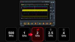
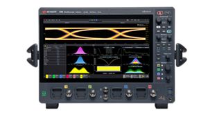
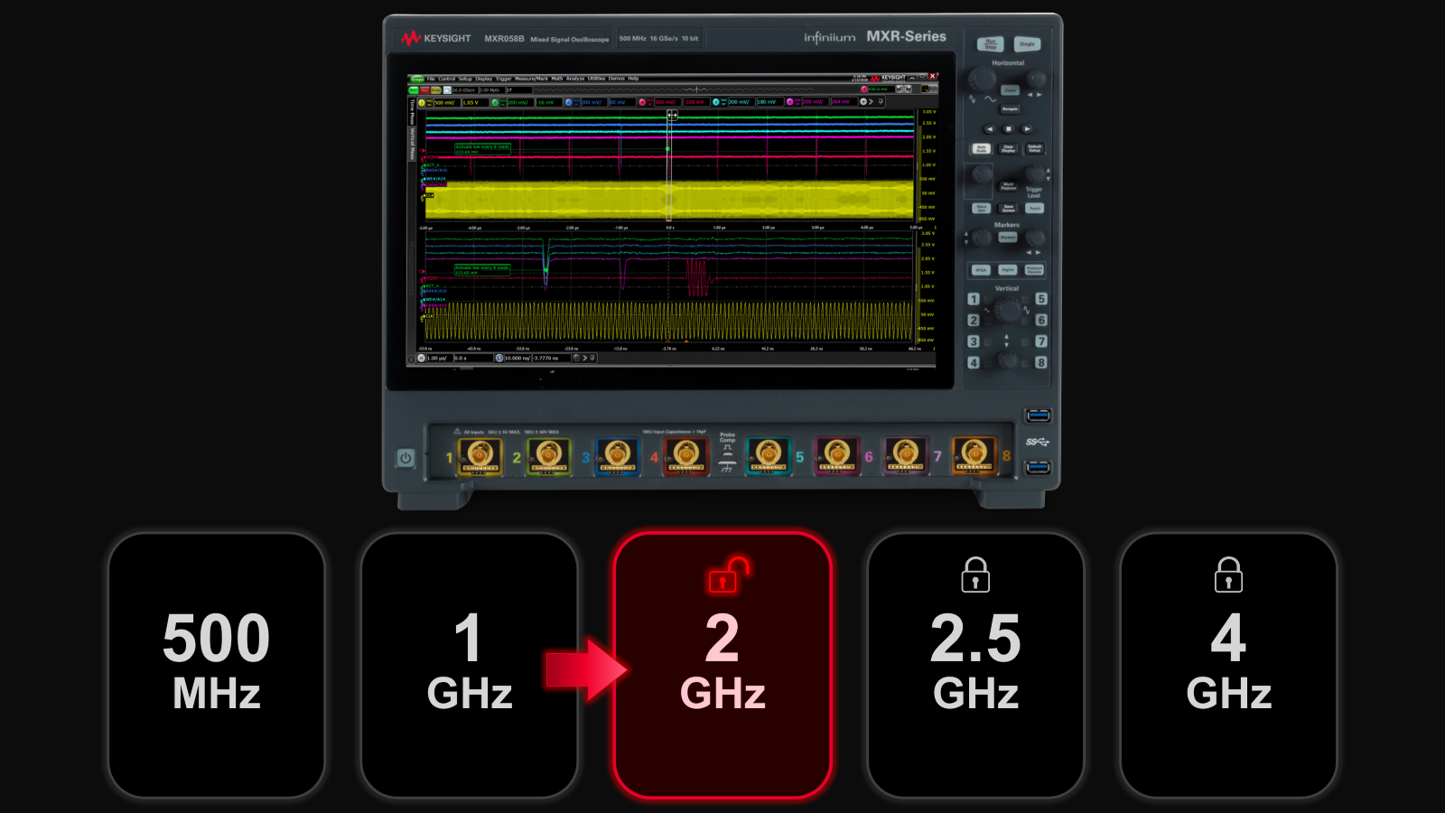
Buy an Expert Oscilloscope, Boost Your Bandwidth
Unlock your free upgrade to the next bandwidth tier.
-
End-to-End Validation for AI Data Center
Strengthen 1.6T network reliability for AI-scale workloads from transceivers to interconnects.

-
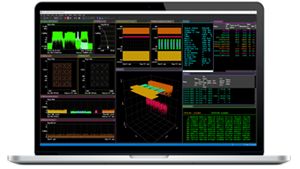
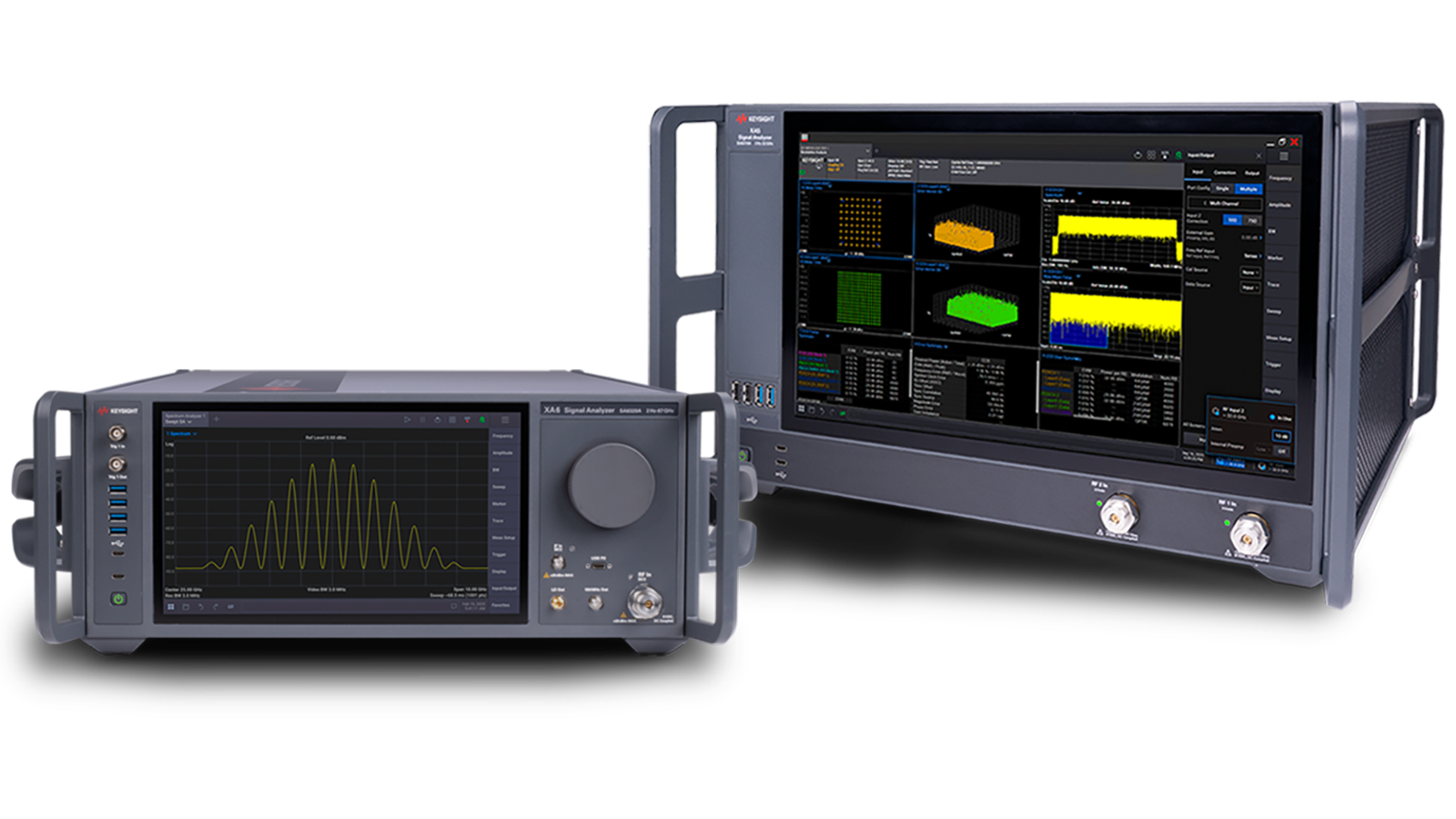
Take On Complex MIMO Signals
Pair Keysight VSA software with the new XA5 signal analyzer for advanced visualization, demodulation, and analysis — start your 30-day trial today.
-
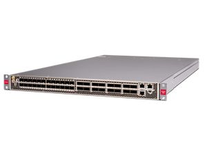
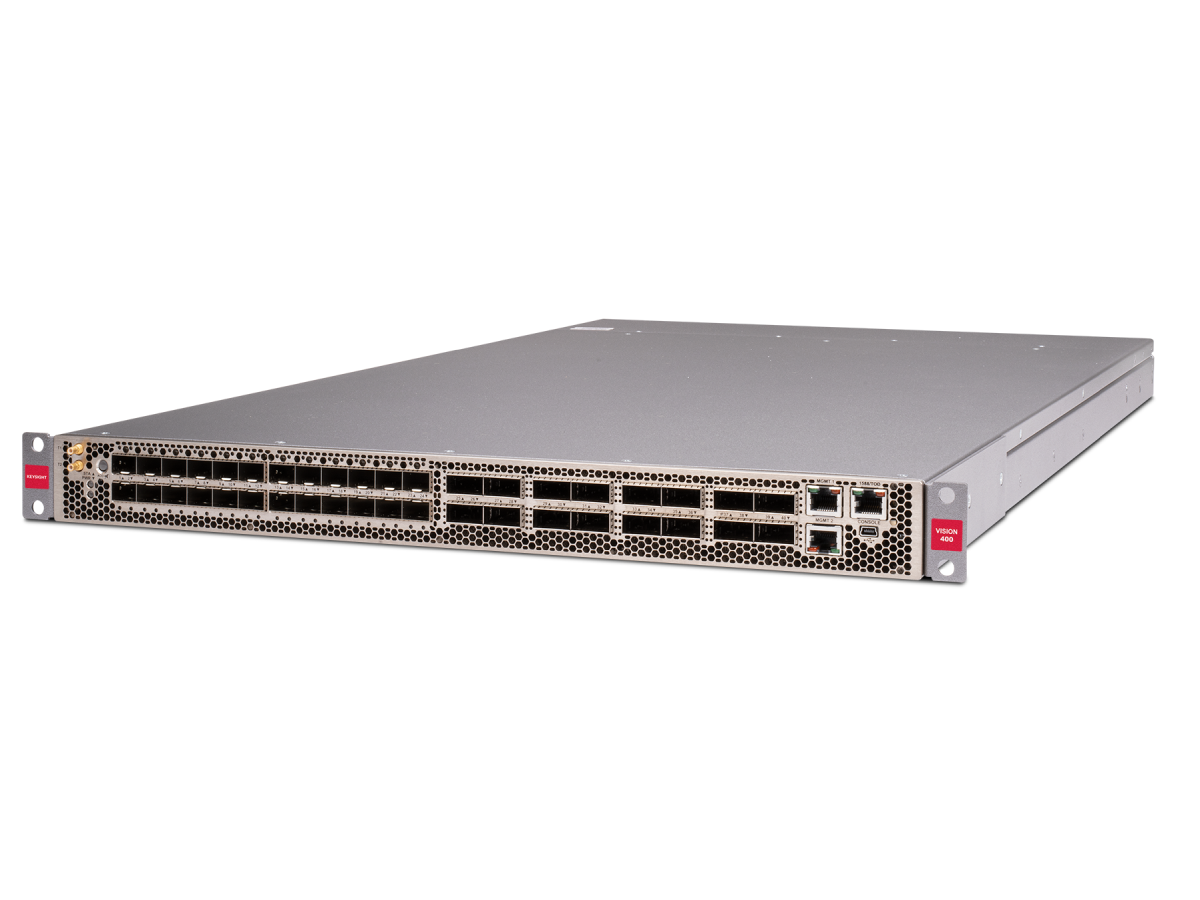
Introducing AI-Enhanced Packet Brokers
With extra memory and storage, these enhanced NPBs run Keysight's AI security and performance monitoring software and AI stack.
-
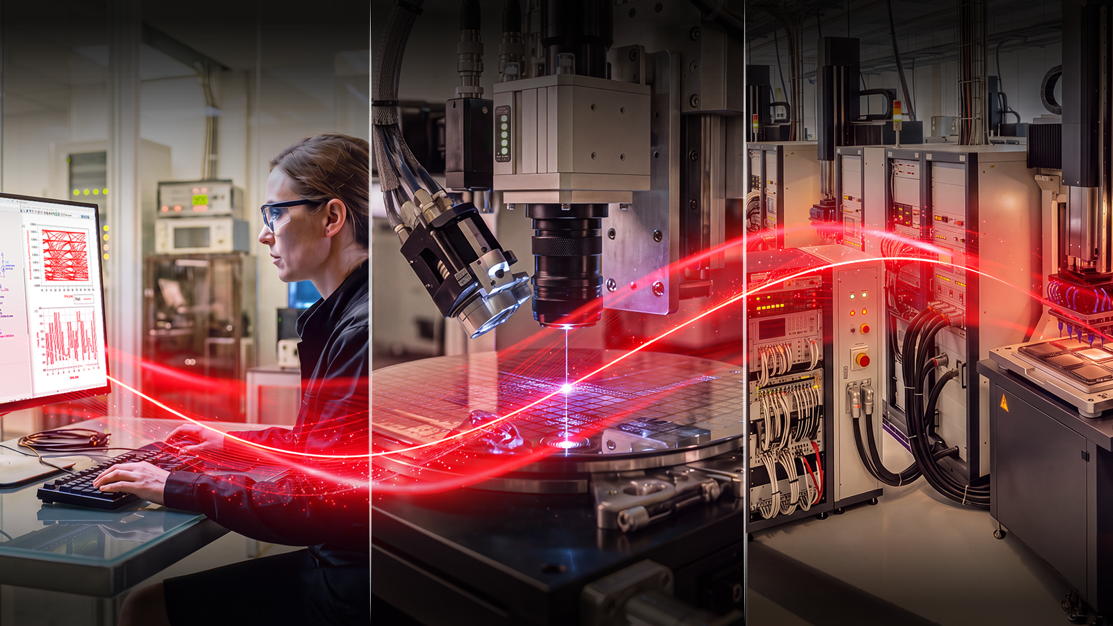
Accelerate Semiconductor Innovation
Explore end-to-end workflows spanning IC design, validation, wafer test, and photonics.
-
Accelerate Your Innovation Engine
Explore curated support plans, prioritized to keep you innovating at speed.

-
-
The Right Connection Makes the Measurement
Maximize accuracy and performance with precision accessories engineered for Keysight instruments.

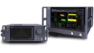
Analyze Complex RF Signals FasterExplore dual-channel and ultra-wideband signal analysis for demanding RF workflows.
 Digital Validation. Faster.
Get faster, clearer insights with our new multicore, 12-bit oscilloscope up to 33 GHz. Trade in your old oscilloscope and get credit toward a new XR8.
-
-
Purpose-built solutions engineered for the design and test challenges unique to your industry.
Use Cases mapped to every stage of your product lifecycle, from design through operations.
Success Stories
HPE Juniper Networking Builds Next-Gen AI Infrastructure -
Authoritative application notes, data sheets, reference designs, and test procedures to accelerate design and validation decisions.
FeaturedHands‑on bootcamps that teach system design, test methods, and production workflows engineers can apply immediately.
Learning Hub
AI TechnologyExplore methodologies, test strategies, and technical resources for designing, validating, and scaling AI systems and networks.
-
Quick access to the most frequent support related self-help tasks.
Additional content to support your product needs.
Do more with Keysight ServicesExplore services to accelerate every step of your innovation journey.








All Software Catalog
Use the filters below to find the software for your specific instrument
Showing 12 of 37
No Filter available
No Filter available
No Filter available
PathWave Manufacturing Analytics
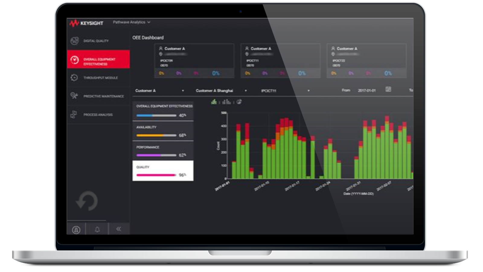
Use PM2288A PathWave Manufacturing Analytics to drive manufacturing improvements with an Industry 4.0 electronics data analytics solution.
Use PM2288A PathWave Manufacturing Analytics to drive manufacturing improvements with an Industry 4.0 electronics data analytics solution.
PathWave Manufacturing Analytics
PM2288A
Use PM2288A PathWave Manufacturing Analytics to drive manufacturing improvements with an Industry 4.0 electronics data analytics solution.
Combining test and measurement expertise with data science and big data engineering, the PathWave Manufacturing Analytics platform provides actionable insights for every level in your organization in the smart factory of the future. Improve yield, lower retest and handling, and lower the cost of poor quality with big data advanced analytics that really works. Accelerate your Return on Investment and business outcomes with unique, innovative analytics.
Descriptive
- View your factory performance in terms of Overall Operating Efficiency (OEE), yield, first pass yield, retest, volume, etc. with extensive drilldowns and filters
- Save the workspace and see your own personalized dashboard on demand, real-time from anywhere
Diagnostic
- Use no-code specially curated diagnostic tools and visualizations for all levels of operators, technicians and engineers
- Root cause issues with just a few clicks, compare between multiple tests, systems, fixtures, parts, probes and more
Predictive
- Predict potential quality issues in real-time manufacturing with optimized machine learning anomaly detection models
- Get only “high severity scored” alerts. Take action to prevent catastrophe and mitigate the risks of poor quality without alert fatigue
Prescriptive
- Prescribe real-time adaptive test limits with optimized dynamic part averaging testing
- Leverage transformed data and insights for horizontal and vertical systems to optimize processes
TestExec SL Software
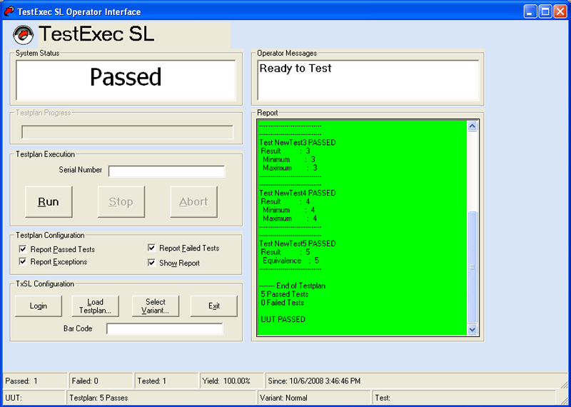
TestExec SL is a highly flexible test executive software for electronics manufacturing functional test applications in multiple industries.
TestExec SL is a highly flexible test executive software for electronics manufacturing functional test applications in multiple industries.
TestExec SL Software
E2011GC
TestExec SL is a highly flexible test executive software for electronics manufacturing functional test applications in multiple industries.
- Intelligent architecture - supports C/C++, VB, C#, VB.NET, Keysight VEE, and more
- Switch Manager - streamlines the task of switching topology configuration
- Test Profiler - evaluates and optimizes the performance throughput of individual tests
- Throughput Multiplier - increases throughput through batch testing for multiple UUTs
- Reusable library - provides framework for code reuse (handlers, actions, and test sequences)
- Multithreading – executes multiple test statements simultaneously
- Operating system Test Exec SL 8.1: Window® 10. Windows® 7 Professional or Home Edition, Service Pack 1 or later
- Operating system Test Exec SL 7.1: Windows® 7 32-bit or 64-bit Professional or Home Edition, Service Pack 1 or later. Windows® XP Professional or Home Edition, Service Pack 2 or later. Windows® 2000 Professional, Service Pack 4 or later
Keysight Technologies' TestExec SL is a customizable, flexible test executive developed specifically for electronics manufacturing functional test applications. This off-the-shelf test executive empowers test developers with a fully customizable operator interface, open architecture for multiple instrument integration, flexible test sequencing, easy debugging tools, and provisions for line integration in most manufacturing test environments. TestExec SL boosts productivity, offers unique advantages for test automation, and is unbeaten for ease of use. With the new release of TestExec SL 7.1, you can utilize the multithreading feature to improve execution throughput and reduce idle time.
User manual and help file for TestExec SL are available in the installation files.
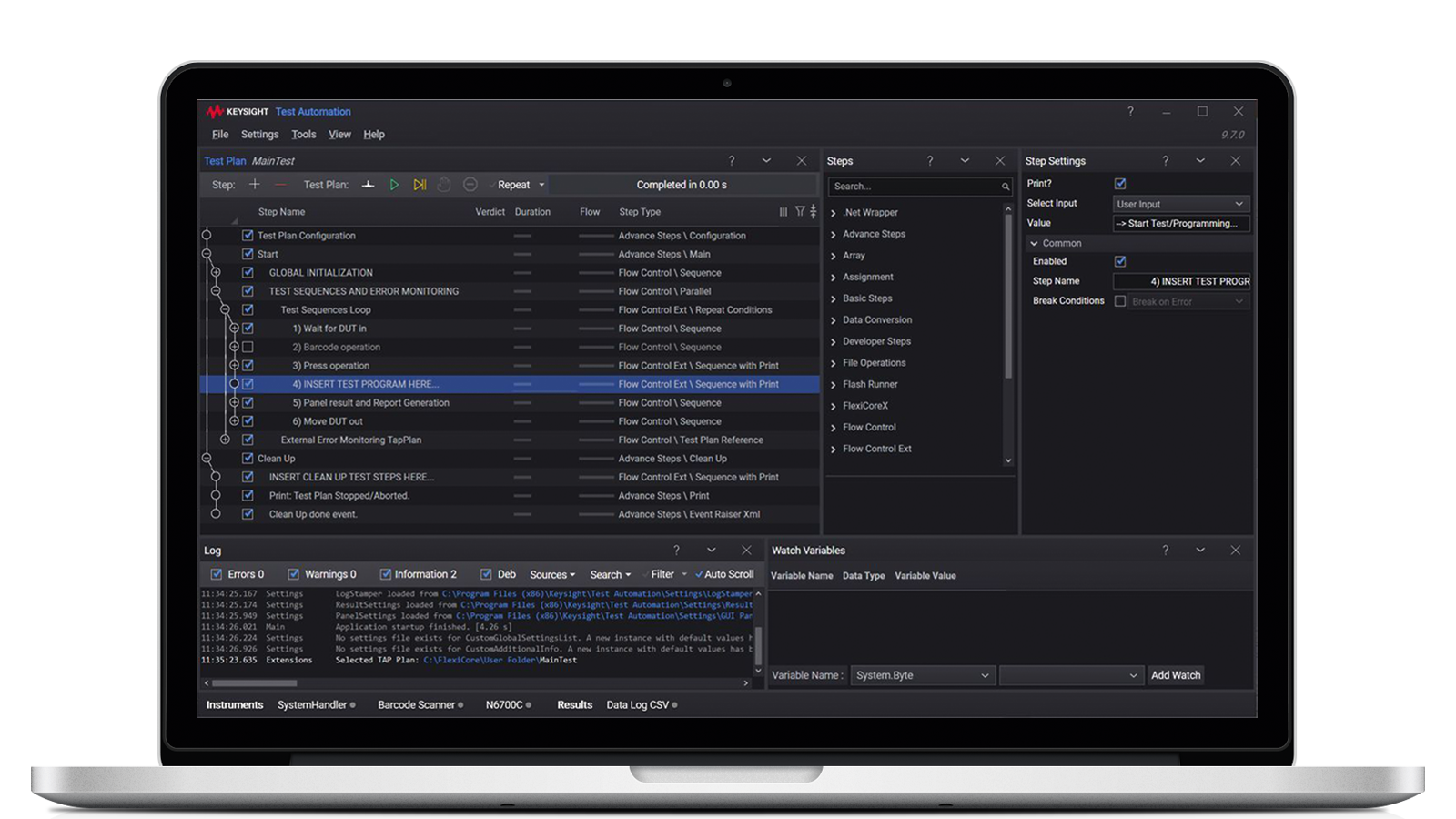
PathWave Test Executive for Manufacturing Developer Version
KS8328A PathWave Test Executive for Manufacturing operates on TAP, fast track automated test plan creation to reduce development time and enhance user experience.
KS8328A PathWave Test Executive for Manufacturing operates on TAP, fast track automated test plan creation to reduce development time and enhance user experience.
PathWave Test Executive for Manufacturing Developer Version
KS8328A
KS8328A PathWave Test Executive for Manufacturing operates on TAP, fast track automated test plan creation to reduce development time and enhance user experience.
PathWave Test Executive for Manufacturing (PTEM) is a plug-in that enhances the user experience in developing automated test programs using PathWave Test Automation Platform (TAP). With powerful PathWave Test Executive software, we eliminate the need to maintain or develop a test platform by users, especially in a manufacturing environment where a high mix of products exist, the maintenance, enhancement, and control of it could become challenging. Development of a test execution platform should not be a priority for valuable resources, instead optimizing and improving test coverage should be the key area of focus.
Prioritize the benefits
- Minimize programming and coding effort, promote code reuse with a common platform
- Create high-level steps, share them and gain the benefits of test standardization for repeatable use cases
- New and improved graphical switch manager, visualizes instrument and switch connections
- Easy learning curve, inexperienced users can quickly get involved with the features and tools available
- Inclusive at no extra cost, a set of library functions for multiple Keysight instruments
- Developer version: KS8328A (Requires KS8400A PathWave Test Automation)
- Deployment version: KS8329A
- Software licenses are available as node-locked, transportable, or floating
- Licenses are available for purchase with 6-, 12-, 24- or 36-month support
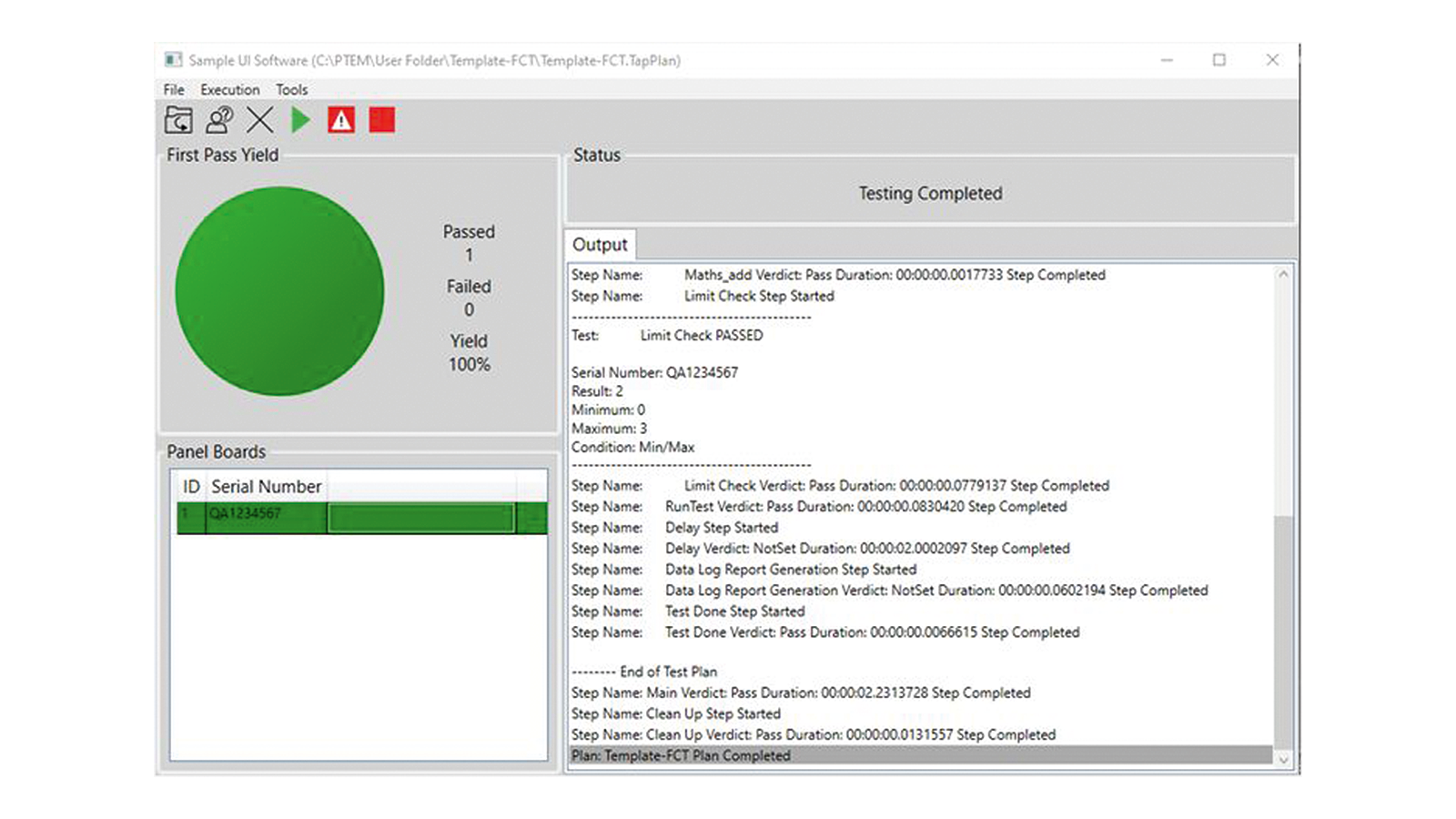
Deploy test plans created with PathWave Test Executive for Manufacturing, deployment and developer licenses provide flexibility in managing cost of test.
Deploy test plans created with PathWave Test Executive for Manufacturing, deployment and developer licenses provide flexibility in managing cost of test.
KS8329A
Deploy test plans created with PathWave Test Executive for Manufacturing, deployment and developer licenses provide flexibility in managing cost of test.
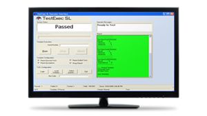

TestExec SL Software
TestExec SL is a highly flexible test executive software for electronics manufacturing functional test applications in multiple industries.
TestExec SL is a highly flexible test executive software for electronics manufacturing functional test applications in multiple industries.
TestExec SL Software
E2011GH
TestExec SL is a highly flexible test executive software for electronics manufacturing functional test applications in multiple industries.
Automate Testing with TestExec SL
- Intelligent architecture - supports C/C++, VB, C#, VB.NET, Keysight VEE, and more
- Switch Manager - streamlines the task of switching topology configuration
- Test Profiler - evaluates and optimizes the performance throughput of individual tests
- Throughput Multiplier - increases throughput through batch testing for multiple UUTs
- Reusable library - provides framework for code reuse (handlers, actions, and test sequences)
- Multithreading – executes multiple test statements simultaneously
- Asynchronous testing capabilities to better optimize test time and utilization
Keysight Technologies' TestExec SL is a customizable, flexible test executive developed specifically for electronics manufacturing functional test applications. This off-the-shelf test executive empowers test developers with a fully customizable operator interface, open architecture for multiple instrument integration, flexible test sequencing, easy debugging tools, and provisions for line integration in most manufacturing test environments. TestExec SL boosts productivity, offers unique advantages for test automation, and is unbeaten for ease of use.
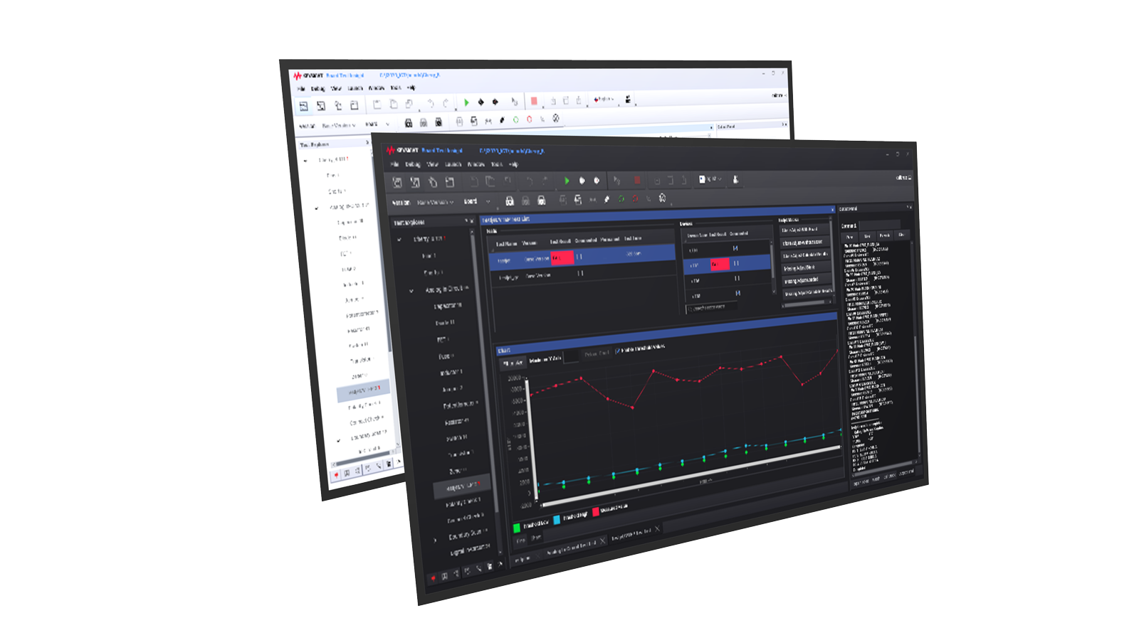
1149.1 Boundary Scan Feature, GTE 10.00p
Boundary scan is a method for testing interconnections on printed circuit boards. Keysight’s Interconnect Plus Boundary Scan feature enables all the tools required to develop and execute this foundational test method on the board under test.
Boundary scan is a method for testing interconnections on printed circuit boards. Keysight’s Interconnect Plus Boundary Scan feature enables all the tools required to develop and execute this foundational test method on the board under test.
1149.1 Boundary Scan Feature, GTE 10.00p
K8212A
Boundary scan is a method for testing interconnections on printed circuit boards. Keysight’s Interconnect Plus Boundary Scan feature enables all the tools required to develop and execute this foundational test method on the board under test.
Boundary scan is a method for testing interconnections on printed circuit boards. Keysight’s Interconnect Plus Boundary Scan feature enables all the tools required to develop and execute this foundational test method on the board under test.
When a number of boundary scan compliant devices are chained together, the Interconnect Plus boundary scan test checks that all the interconnecting pins on the devices within the chain are making electrical contact with the printed circuit board.
When the Interconnect Plus Boundary Scan feature is enabled, the powered shorts, interconnect, bus wire, connect, and chain disable tests are automatically generated according to the IEEE 1149.1 standards with the test patterns defined for the most efficient and complete test coverage for the devices under test.
1149.1 Boundary Scan Feature, GTE 10.00p
Boundary scan is a method for testing interconnections on printed circuit boards. Keysight’s Interconnect Plus Boundary Scan feature enables all the tools required to develop and execute this foundational test method on the board under test.
Boundary scan is a method for testing interconnections on printed circuit boards. Keysight’s Interconnect Plus Boundary Scan feature enables all the tools required to develop and execute this foundational test method on the board under test.
1149.1 Boundary Scan Feature, GTE 10.00p
K8212B
Boundary scan is a method for testing interconnections on printed circuit boards. Keysight’s Interconnect Plus Boundary Scan feature enables all the tools required to develop and execute this foundational test method on the board under test.
Boundary scan is a method for testing interconnections on printed circuit boards. Keysight’s Interconnect Plus Boundary Scan feature enables all the tools required to develop and execute this foundational test method on the board under test.
When a number of boundary scan compliant devices are chained together, the Interconnect Plus boundary scan test checks that all the interconnecting pins on the devices within the chain are making electrical contact with the printed circuit board.
When the Interconnect Plus Boundary Scan feature is enabled, the powered shorts, interconnect, buswire, connect, and chain disable tests are automatically generated according to the IEEE 1149.1 standards with the test patterns defined for the most efficient and complete test coverage for the devices under test.
1149.6 Boundary Scan Feature, GTE 10.00p
Keysight’s Interconnect Plus Boundary Scan 1149.6 feature enables all the tools required to develop and execute this test method on the board under test. Compared to the 1149.1 standards, the 1149.6 standards define test methods for the boundary scan devices that are designed with AC coupled signals or differential nets needed for high-speed operations of the device.
Keysight’s Interconnect Plus Boundary Scan 1149.6 feature enables all the tools required to develop and execute this test method on the board under test. Compared to the 1149.1 standards, the 1149.6 standards define test methods for the boundary scan devices that are designed with AC coupled signals or differential nets needed for high-speed operations of the device.
1149.6 Boundary Scan Feature, GTE 10.00p
K8213A
Keysight’s Interconnect Plus Boundary Scan 1149.6 feature enables all the tools required to develop and execute this test method on the board under test. Compared to the 1149.1 standards, the 1149.6 standards define test methods for the boundary scan devices that are designed with AC coupled signals or differential nets needed for high-speed operations of the device.
Boundary scan is a method for testing interconnections on printed circuit boards. Keysight’s Interconnect Plus Boundary Scan 1149.6 feature enables all the tools required to develop and execute this test method on the board under test. Compared to the 1149.1 standards, the 1149.6 standards define test methods for boundary scan devices that are designed with AC coupled signals or differential nets needed for high-speed operations of the device.
When enabled, the Interconnect Plus Boundary Scan 1149.6 development tools will automatically generate the 1149.6 tests when 1149.6 compliant devices are detected on the printed circuit board.
Keysight has the most comprehensive test patterns for 1149.6 testing. Defects such as shorts or opens on the differential pins and missing coupling capacitors can be detected.
1149.6 Boundary Scan Feature, GTE 10.00p
Keysight’s Interconnect Plus Boundary Scan 1149.6 feature enables all the tools required to develop and execute this test method on the board under test. Compared to the 1149.1 standards, the 1149.6 standards define test methods for the boundary scan devices that are designed with AC coupled signals or differential nets needed for high-speed operations of the device.
Keysight’s Interconnect Plus Boundary Scan 1149.6 feature enables all the tools required to develop and execute this test method on the board under test. Compared to the 1149.1 standards, the 1149.6 standards define test methods for the boundary scan devices that are designed with AC coupled signals or differential nets needed for high-speed operations of the device.
1149.6 Boundary Scan Feature, GTE 10.00p
K8213B
Keysight’s Interconnect Plus Boundary Scan 1149.6 feature enables all the tools required to develop and execute this test method on the board under test. Compared to the 1149.1 standards, the 1149.6 standards define test methods for the boundary scan devices that are designed with AC coupled signals or differential nets needed for high-speed operations of the device.
Boundary scan is a method for testing interconnections on printed circuit boards. Keysight’s Interconnect Plus Boundary Scan 1149.6 feature enables all the tools required to develop and execute this test method on the board under test. Compared to the 1149.1 standards, the 1149.6 standards define test methods for boundary scan devices that are designed with AC coupled signals or differential nets needed for high-speed operations of the device.
When enabled, the Interconnect Plus Boundary Scan 1149.6 development tools will automatically generate the 1149.6 tests when 1149.6 compliant devices are detected on the printed circuit board.
Keysight has the most comprehensive test patterns for 1149.6 testing. Defects such as shorts or opens on the differential pins and missing coupling capacitors can be detected.
Silicon Nails Feature, GTE 10.00p
Keysight’s Silicon Nails feature enables all the tools required to develop and execute tests on non-compliant boundary scan devices that are connected to boundary scan compliant devices on the printed circuit board.
Keysight’s Silicon Nails feature enables all the tools required to develop and execute tests on non-compliant boundary scan devices that are connected to boundary scan compliant devices on the printed circuit board.
Silicon Nails Feature, GTE 10.00p
K8214A
Keysight’s Silicon Nails feature enables all the tools required to develop and execute tests on non-compliant boundary scan devices that are connected to boundary scan compliant devices on the printed circuit board.
Boundary scan is a method for testing interconnections on printed circuit boards. Keysight’s Silicon Nails feature enables all the tools required to develop and execute tests on non-compliant boundary scan devices that are connected to boundary scan compliant devices on the printed circuit board.
During test development, the Silicon Nails test development tool references the digital test defined for the non-compliant boundary scan device. Then, it will generate a boundary scan test that drives the boundary scan devices on the chain to execute the test vectors on the non-compliant boundary scan device. So, the tester is driving the non-compliant boundary scan device and testing it through the boundary scan chain.
The Silicon Nails test development tool also allows users to define the vectors that they would like to execute on the non-compliant boundary scan device. The test development tool will generate the boundary scan test to output or input at the relevant interconnecting pin, thus generating the test consistently.
Silicon Nails Feature, GTE 10.00p
Keysight’s Silicon Nails feature enables all the tools required to develop and execute tests on non-compliant boundary scan devices that are connected to boundary scan compliant devices on the printed circuit board.
Keysight’s Silicon Nails feature enables all the tools required to develop and execute tests on non-compliant boundary scan devices that are connected to boundary scan compliant devices on the printed circuit board.
Silicon Nails Feature, GTE 10.00p
K8214B
Keysight’s Silicon Nails feature enables all the tools required to develop and execute tests on non-compliant boundary scan devices that are connected to boundary scan compliant devices on the printed circuit board.
Boundary scan is a method for testing interconnections on printed circuit boards. Keysight’s Silicon Nails feature enables all the tools required to develop and execute tests on non-compliant boundary scan devices that are connected to boundary scan compliant devices on the printed circuit board.
During test development, the Silicon Nails test development tool references the digital test defined for the non-compliant boundary scan device. Then, it will generate a boundary scan test that drives the boundary scan devices on the chain to execute the test vectors on the non-compliant boundary scan device. So, the tester is driving the non-compliant boundary scan device and testing it through the boundary scan chain.
The Silicon Nails test development tool also allows users to define the vectors that they would like to execute on the non-compliant boundary scan device. The test development tool will generate the boundary scan test to output or input at the relevant interconnecting pin, thus generating the test consistently.
Advanced Throughput Multiplier Feature, GTE 10.00p
The Advanced Throughput Multiplier feature allows you to test up to two 1000 to 2000 node (between 1296 and 2592 nodes) boards simultaneously on a 4 module tester, thus dividing the test time by half.
The Advanced Throughput Multiplier feature allows you to test up to two 1000 to 2000 node (between 1296 and 2592 nodes) boards simultaneously on a 4 module tester, thus dividing the test time by half.
Advanced Throughput Multiplier Feature, GTE 10.00p
K8215A
The Advanced Throughput Multiplier feature allows you to test up to two 1000 to 2000 node (between 1296 and 2592 nodes) boards simultaneously on a 4 module tester, thus dividing the test time by half.
The i3070 In-Circuit Test System architecture is split into 4 modules. Each module can execute tests in parallel with the rest, so you can test 4 printed circuit boards at one time.
For cases when you need to test homogeneous (identical) boards with more than 1000 nodes each, you can combine 2 modules together using the Advanced Throughput Multiplier feature. This allows you to test up to two 1000 to 2000 node (between 1296 and 2592 nodes) boards simultaneously on a 4 module tester, thus dividing the test time by half.
