Choose a country or area to see content specific to your location
何をお探しですか?
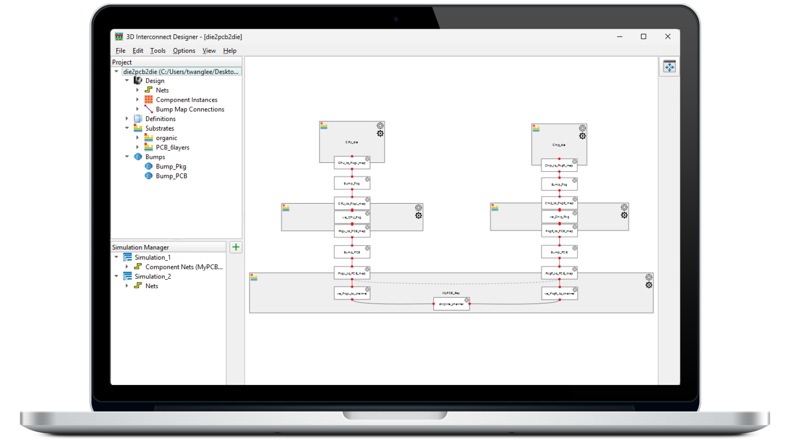
Design, model, and validate complex 3D interconnect architectures with a powerful standalone design environment.
Automate transmitter and receiver validation across next-generation I/O, memory, and fabric interfaces.
Strengthen 1.6T network reliability for AI-scale workloads from transceivers to interconnects.

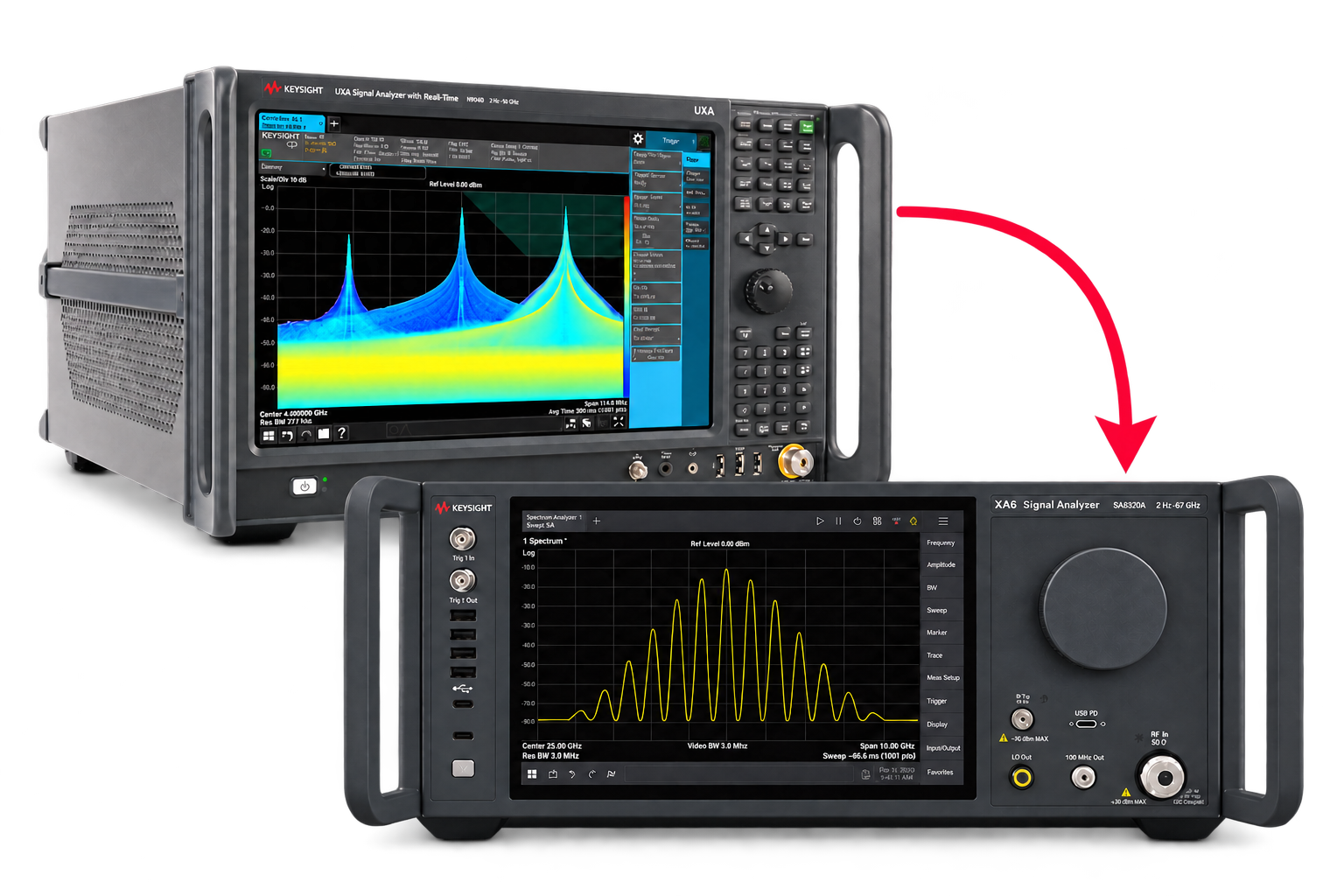
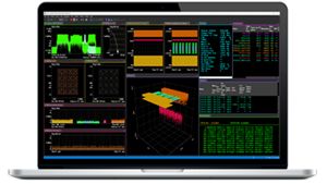
Pair Keysight VSA software with the new XA5 signal analyzer for advanced visualization, demodulation, and analysis — start your 30-day trial today.
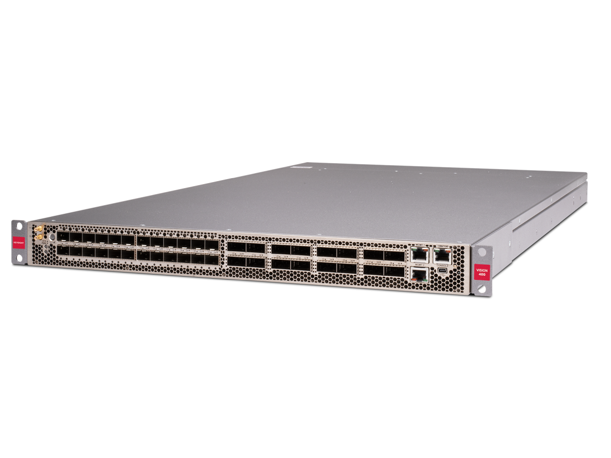
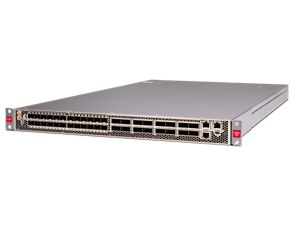
With extra memory and storage, these enhanced NPBs run Keysight's AI security and performance monitoring software and AI stack.
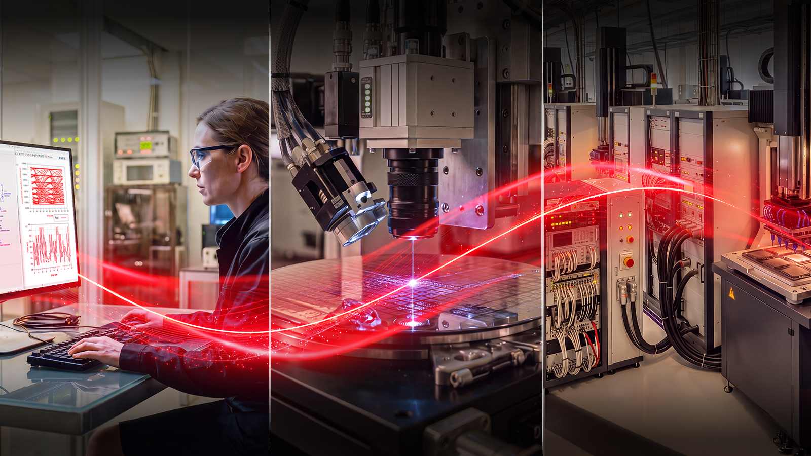
Explore end-to-end workflows spanning IC design, validation, wafer test, and photonics.
Save up to 50% on our latest instruments with eligible Keysight or competitor trade-ins.
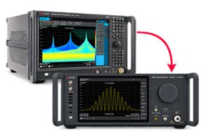
Maximize accuracy and performance with precision accessories engineered for Keysight instruments.
Save up to 50% on our latest instruments with eligible Keysight or competitor trade-ins.
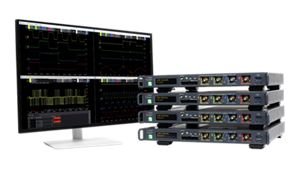
Four channels per 1U of rack space, up to 1 GHz bandwidth, and multi-oscilloscope synchronization.
Purpose-built solutions engineered for the design and test challenges unique to your industry.
Use Cases mapped to every stage of your product lifecycle, from design through operations.
Success Stories
Authoritative application notes, data sheets, reference designs, and test procedures to accelerate design and validation decisions.
Hands‑on bootcamps that teach system design, test methods, and production workflows engineers can apply immediately.
Learning Hub
Explore methodologies, test strategies, and technical resources for designing, validating, and scaling AI systems and networks.
頻繁にお問い合わせされるサポート関連のお役に立つ情報すばやくアクセス
お持ちの製品をサポートするための追加情報
Design, simulate, and optimize photonic devices, PICs, and optical systems with a unified workflow from component physics to system performance.
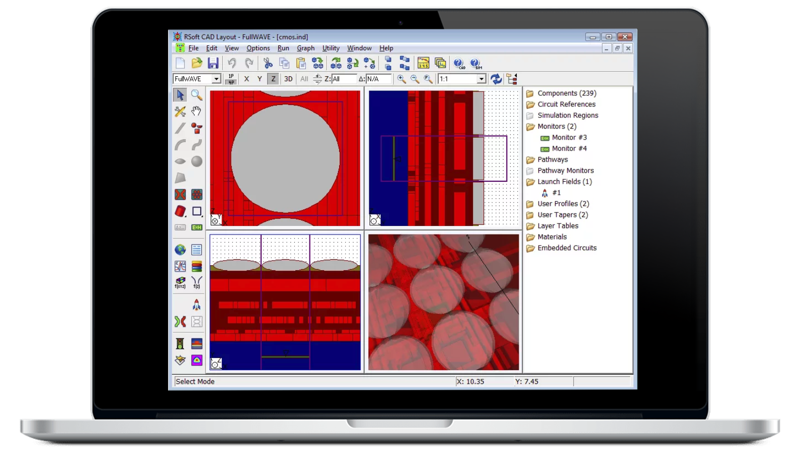
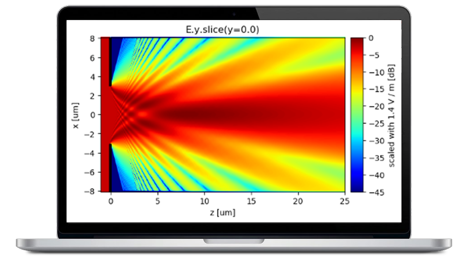
Simulate passive and active photonic components, lasers, and PICs with advanced optical solvers to improve performance and shorten development cycles.
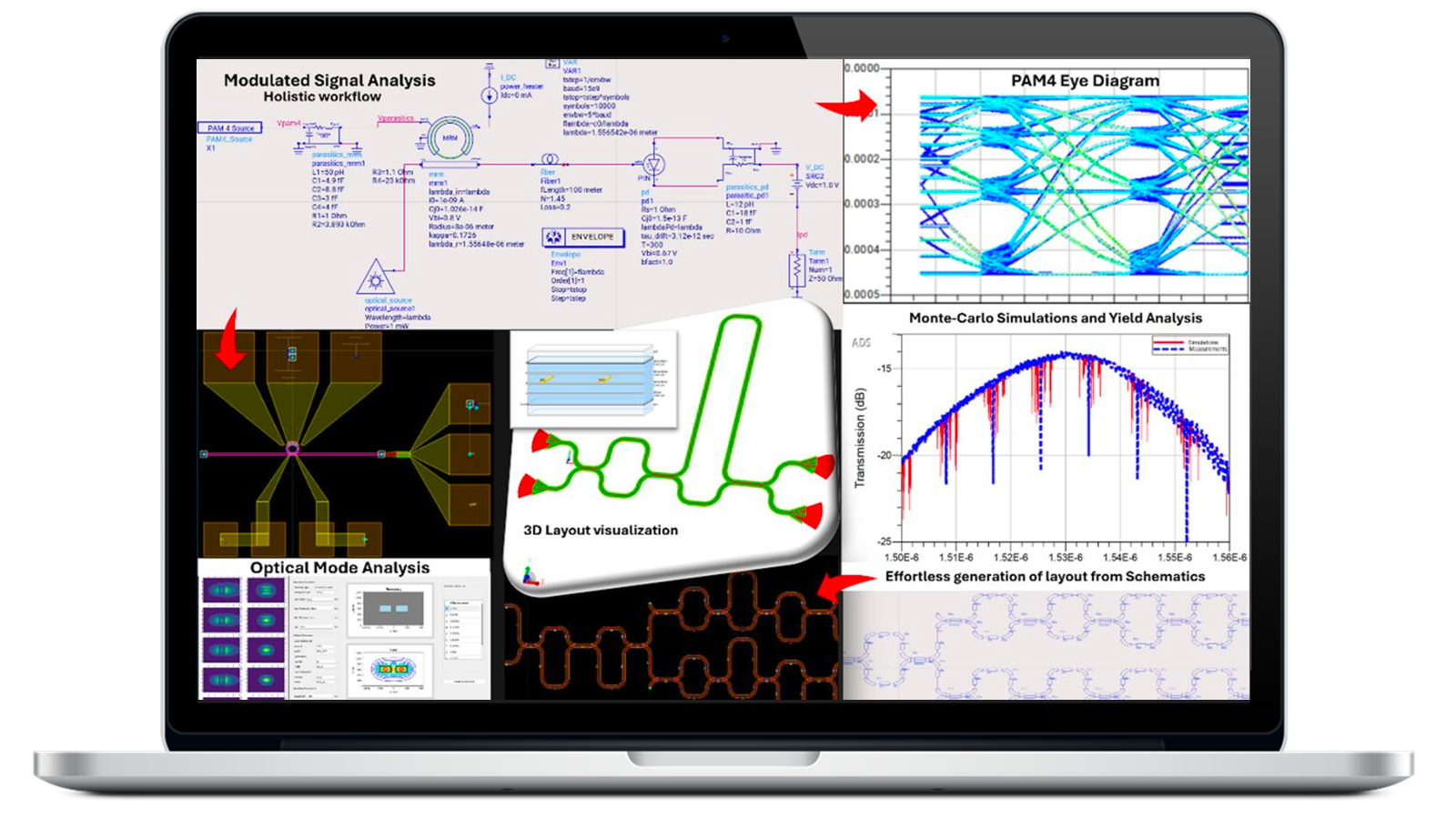
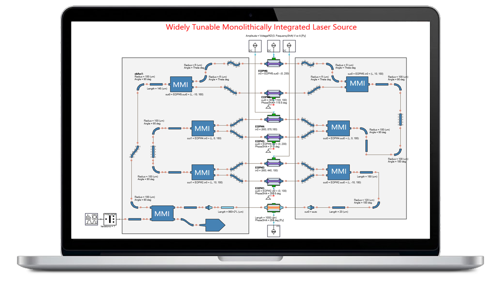
Explore and optimize silicon photonics, indium phosphide, and hybrid PIC designs using circuit-level simulation and comprehensive device libraries.
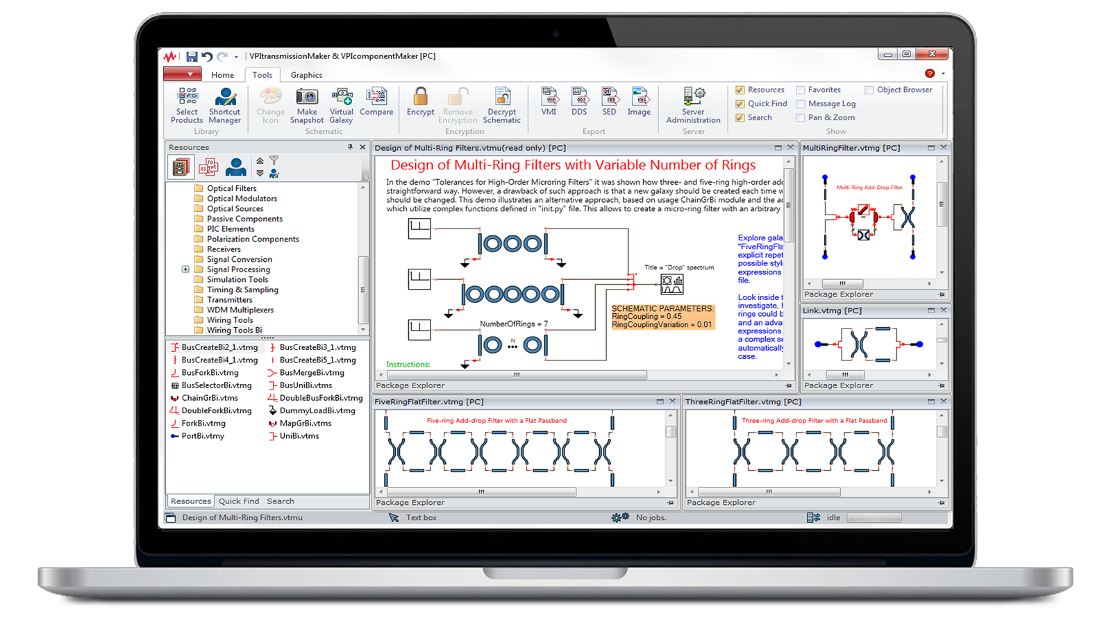
Design optical, electro-optical, and optoelectronic circuits in a single environment with advanced simulation and layout capabilities.
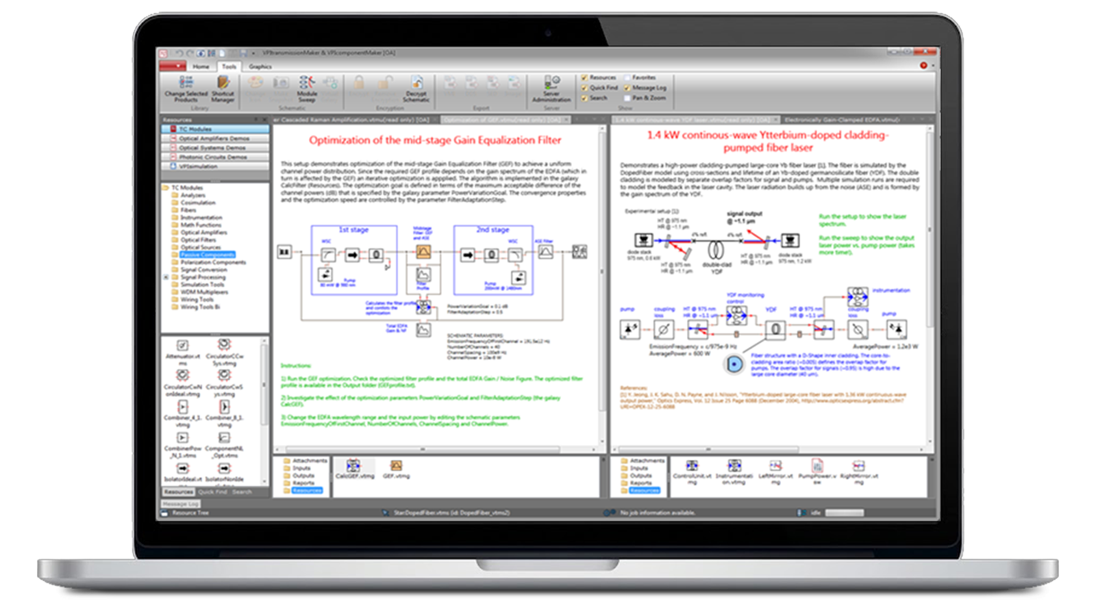
Model, optimize, and validate fiber amplifiers and laser architectures to improve gain, efficiency, noise performance, and power scaling before prototyping.
Simulate and optimize integrated photonic devices, waveguides, and optical fibers with advanced electromagnetic modeling for faster, more accurate photonic design.
(VPItoolkit PDK <fab>)
Accelerate photonic IC development with layout-aware PDK-driven design.
Connect device, circuit, fiber, and system simulations in a flexible environment that streamlines photonic design and optimization.
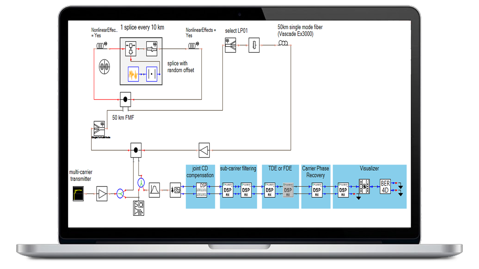
Model and optimize optical links, networks, and subsystems with accurate system-level simulation to accelerate photonic innovation and deployment.
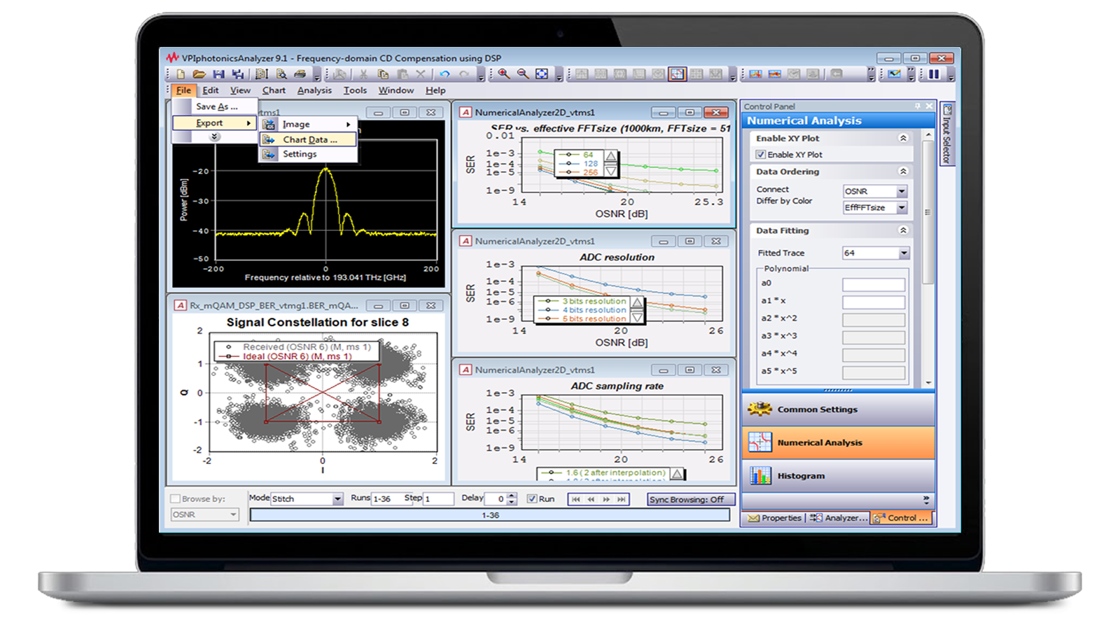
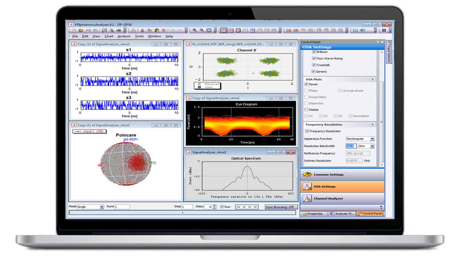
Generate realistic test signals and automate analysis to verify photonic components, subsystems, and transmission systems faster.
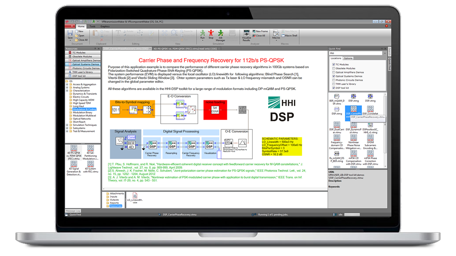
Apply lab-proven DSP algorithms to optimize modulation, compensate transmission impairments, and improve photonic system performance before deployment.
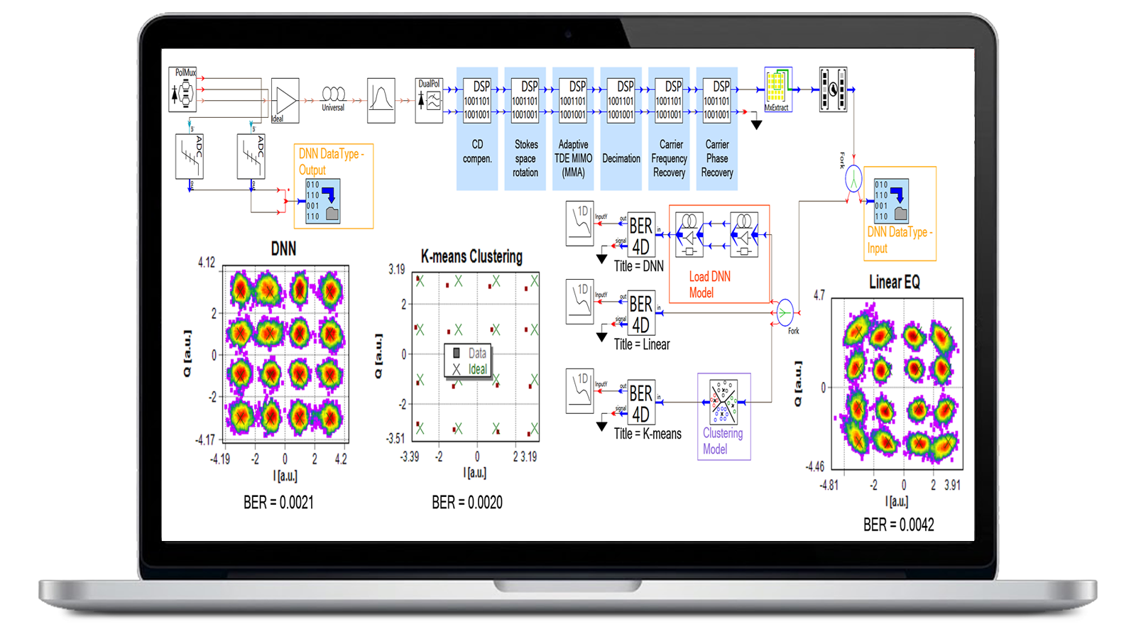
Deploy machine learning algorithms to automate photonic simulation, optimize device behavior, and accelerate design-space exploration.
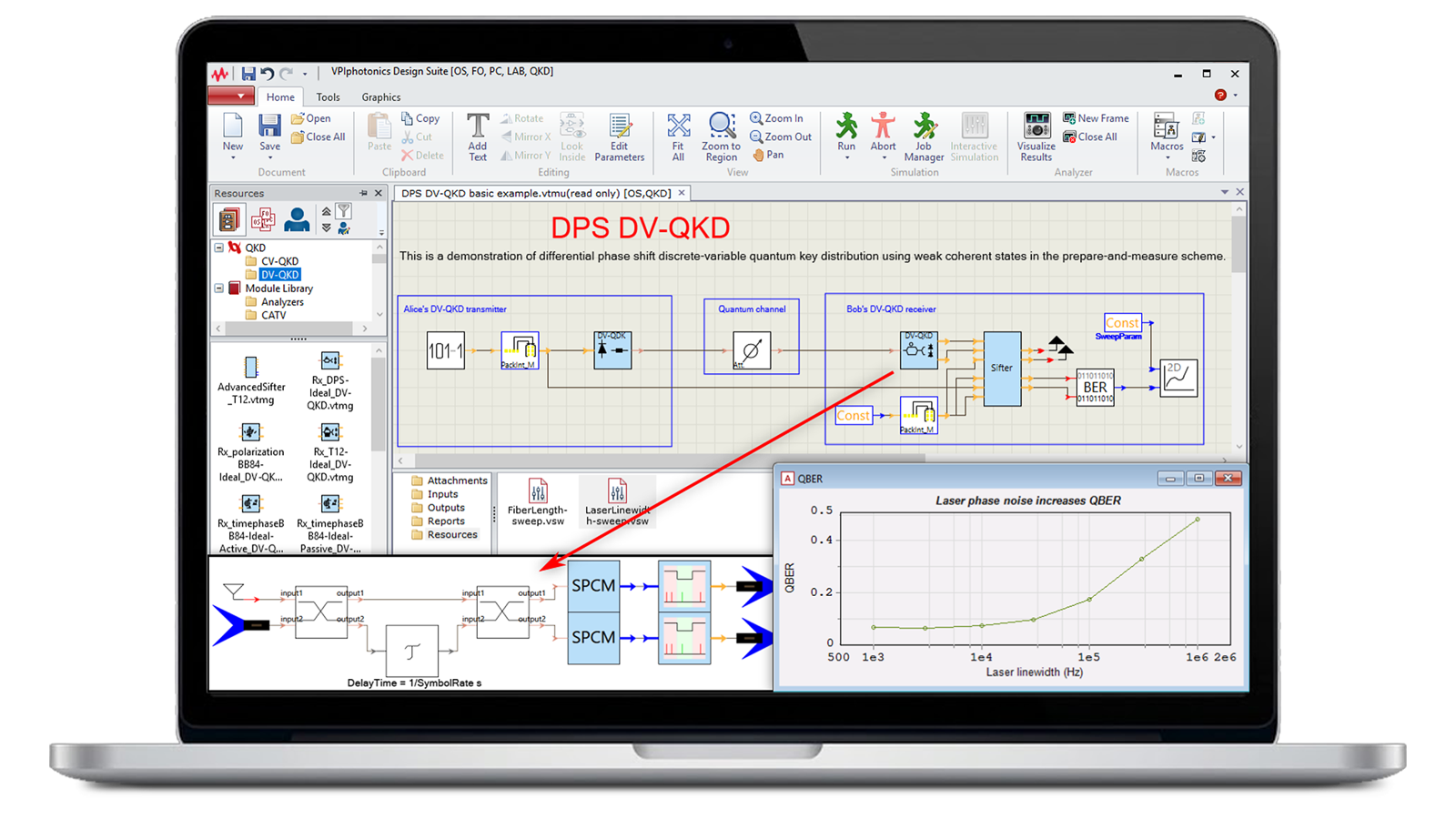
Simulate and optimize quantum key distribution systems, evaluating security, transmission performance, and component impairments before deployment.
Connect device, circuit, fiber, and system simulations in a flexible environment that streamlines photonic design and optimization.
Evaluate OSNR, dispersion, nonlinear effects, and equipment choices to create cost-effective, high-performance optical networks.
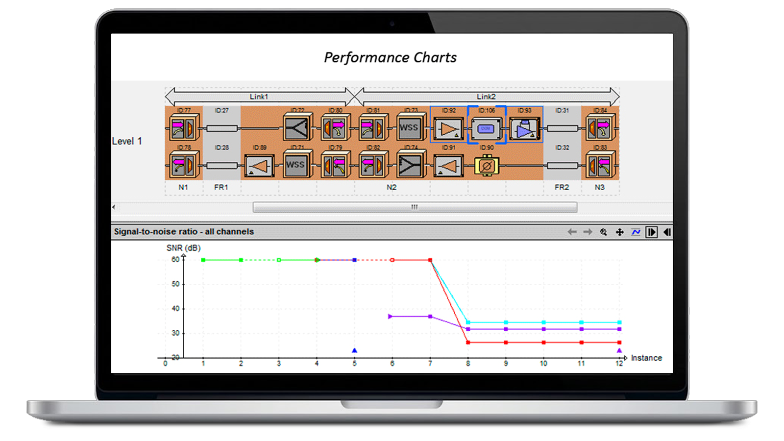
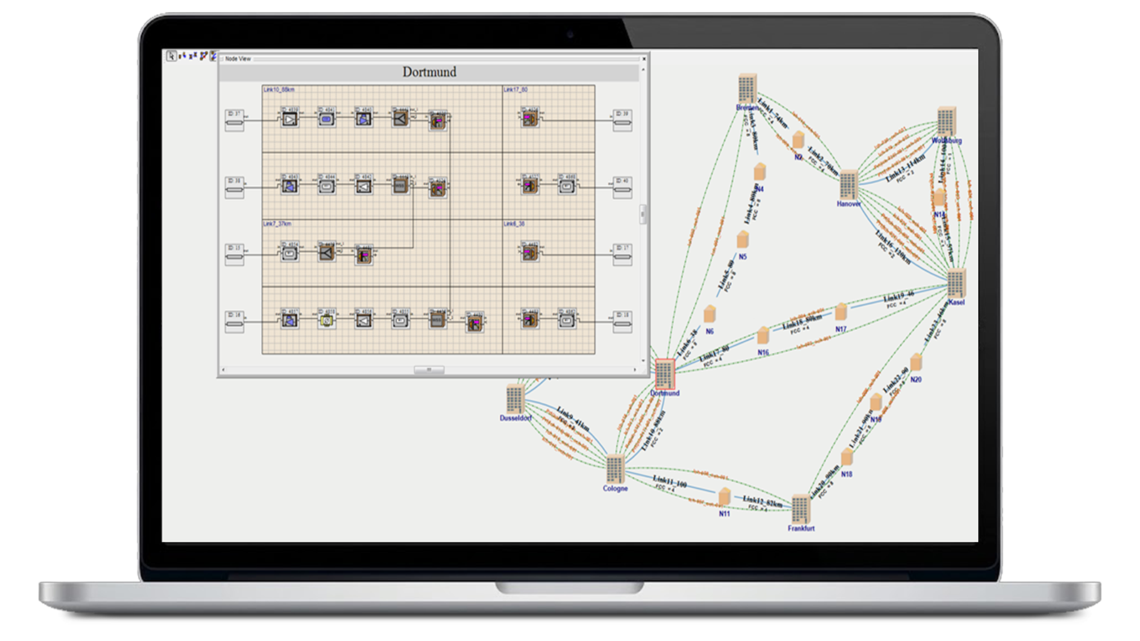
Create and evaluate DWDM, ring, mesh, and point-to-point networks with real-time performance analysis and automated engineering workflows
This brochure presents Keysight’s VPIphotonics portfolio for end-to-end photonic design automation. It covers tools for integrated photonic circuits, optical devices, fiber amplifiers and lasers, transmission systems, and network planning. Key capabilities include interactive simulation, automated optimization, scripting, accelerated computing, and data visualization. Interfaces with third-party software and laboratory equipment support collaborative workflows, while protected model sharing enables design exchange without exposing proprietary information.
blogs
blogs
blogs
blogs
blogs
アプリケーションノート
Case Studies
アプリケーションノート
アプリケーションノート
WEBINARS
Photonics EDA (Electronic Design Automation) software enables engineers to design, simulate, optimize, and verify photonic devices, photonic integrated circuits, optical subsystems, and complete communication systems before fabrication and deployment.
The portfolio includes solutions for photonic device simulation, PIC design and verification, and system-level optical simulation, enabling workflows that span from component physics to complete optical links.
Photonic Designer is best suited for photonic integrated circuit design, layout-driven workflows, circuit verification, foundry PDK integration, and PIC implementation. It focuses on creating and validating PIC architectures before manufacturing.
Photonic Simulation Environment is ideal for modeling and optimizing optical systems, subsystems, transmission networks, fiber-optic components, and complex electro-optical interactions where overall system performance is the primary concern.
Photonic Designer focuses on circuit-level PIC implementation and verification, while the Photonic Simulation Environment extends analysis to subsystem and system-level behavior. Together they provide continuous design insight from photonic circuits to complete optical links.
Yes. The solutions support multi-domain modeling that incorporates photonic, electrical, and optoelectronic behavior, helping engineers understand how devices and circuits perform within larger systems.
Common applications include datacenter interconnects, coherent optical communications, silicon photonics, co-packaged optics, fiber sensing, laser communications, telecommunications networks, and advanced PIC-based systems.
Yes. The platform supports PDK-driven development and reusable photonic building blocks, helping teams move efficiently from design concepts to manufacturable PIC implementations.
By enabling virtual prototyping, performance verification, and end-to-end system evaluation before fabrication, engineers can identify issues earlier, reduce prototype iterations, and accelerate time-to-market.
Choose Photonic Designer when your priority is PIC architecture, layout, and verification. Choose Photonic Simulation Environment when your priority is subsystem, transmission, or network performance. Many organizations use both to create a complete photonic development workflow from device to system.
Talk to our team to find the right solution for your design needs, get a personalized quote, or request a free trial.
何をお探しですか?