Simulation Software for RTL and Packaging Design
Integrated simulation workflows for ICs (Quantum, Photonic, RFICs and MMICs), device SI/PI interconnects, electro-thermal co-simulation, and Advanced Packaging for Chiplets and 3D Heterogenous Integrations (3DHI).



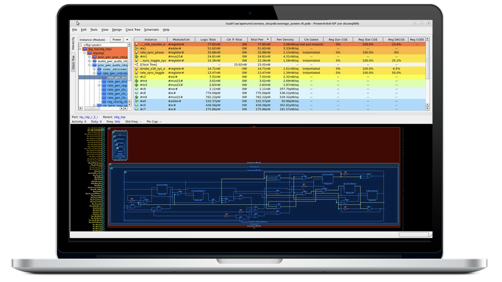
Analyze, profile, and optimize SoC power consumption at the RTL stage, identifying hotspots, improving efficiency, and enabling informed architectural decisions early.

Design leading edge RF, milli-meter wave, and Quantum ICs with a library of supporting Process Design Kits (PDKs).


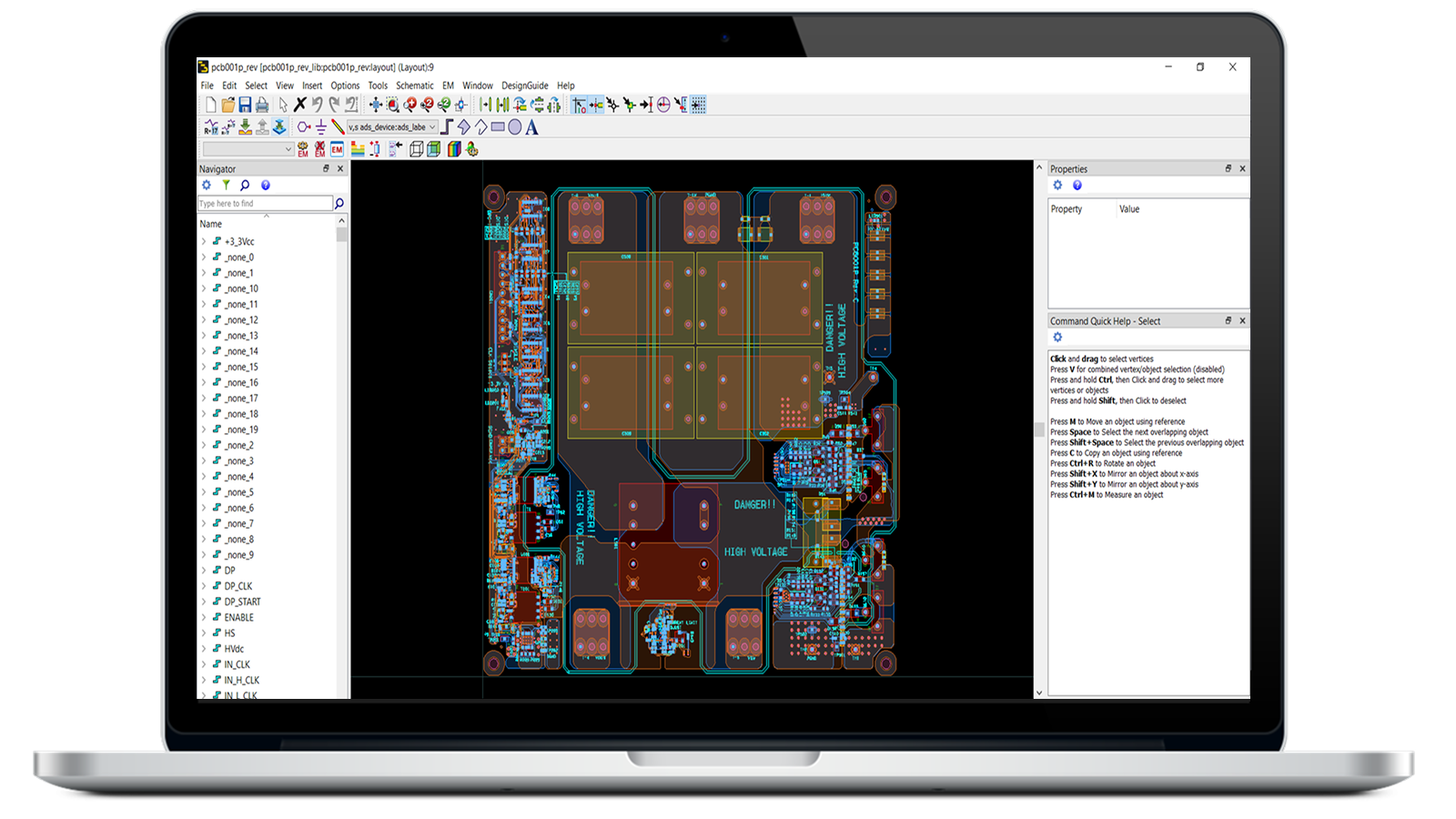
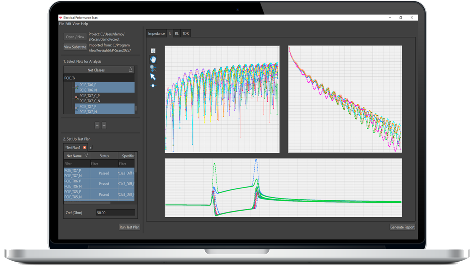
Design and verify high-speed interconnects with advanced signal and power integrity analysis, ensuring compliance, minimizing risk, and improving first-pass PCB success.


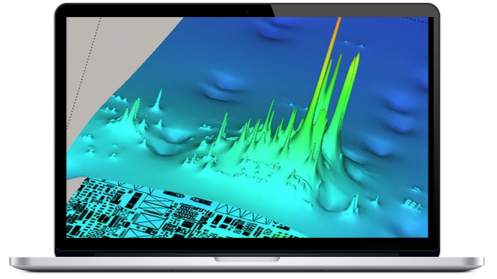
Analyze electrical and thermal interactions simultaneously to predict temperature-dependent behavior, improve reliability, identify hotspots, and optimize high-performance RF and IC designs.

Model Silicon Carbide-based power converters and inverters with EM-circuit co-simulation, thermal analysis, and parasitic-aware workflows to improve efficiency, reliability, and design accuracy.

Dense design integration into one 3D physical structure requires a shared database that spans technology boundaries and hierarchies so that revisions can be traced across the design.
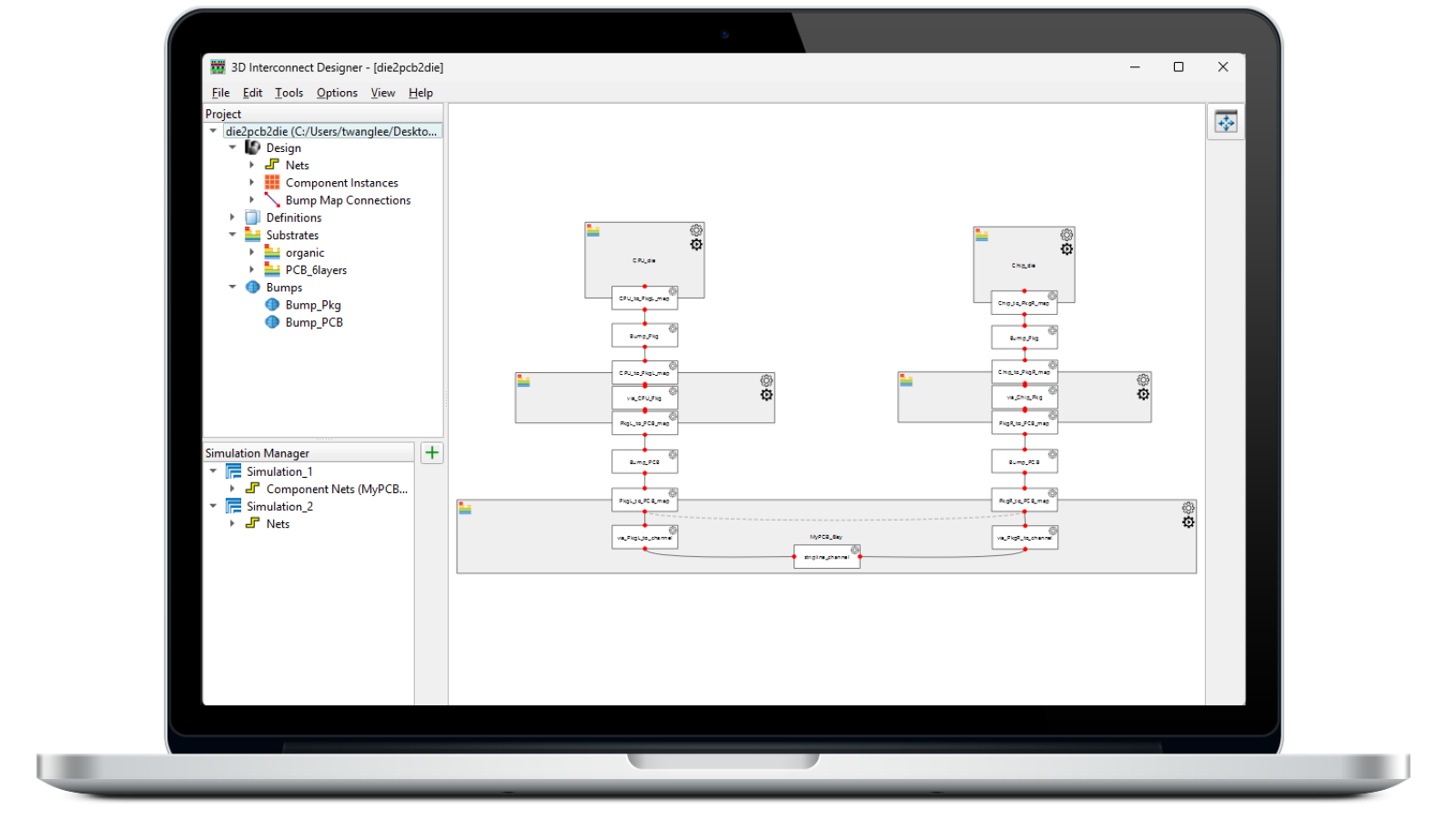
Model, optimize, and validate chiplet and 3DIC interconnects early, improving performance, reducing risk, and accelerating advanced package development.
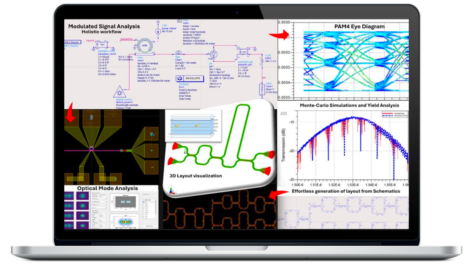
Connect photonic device, PIC, electronic, packaging, and system-level design decisions for emerging optical I/O architectures.

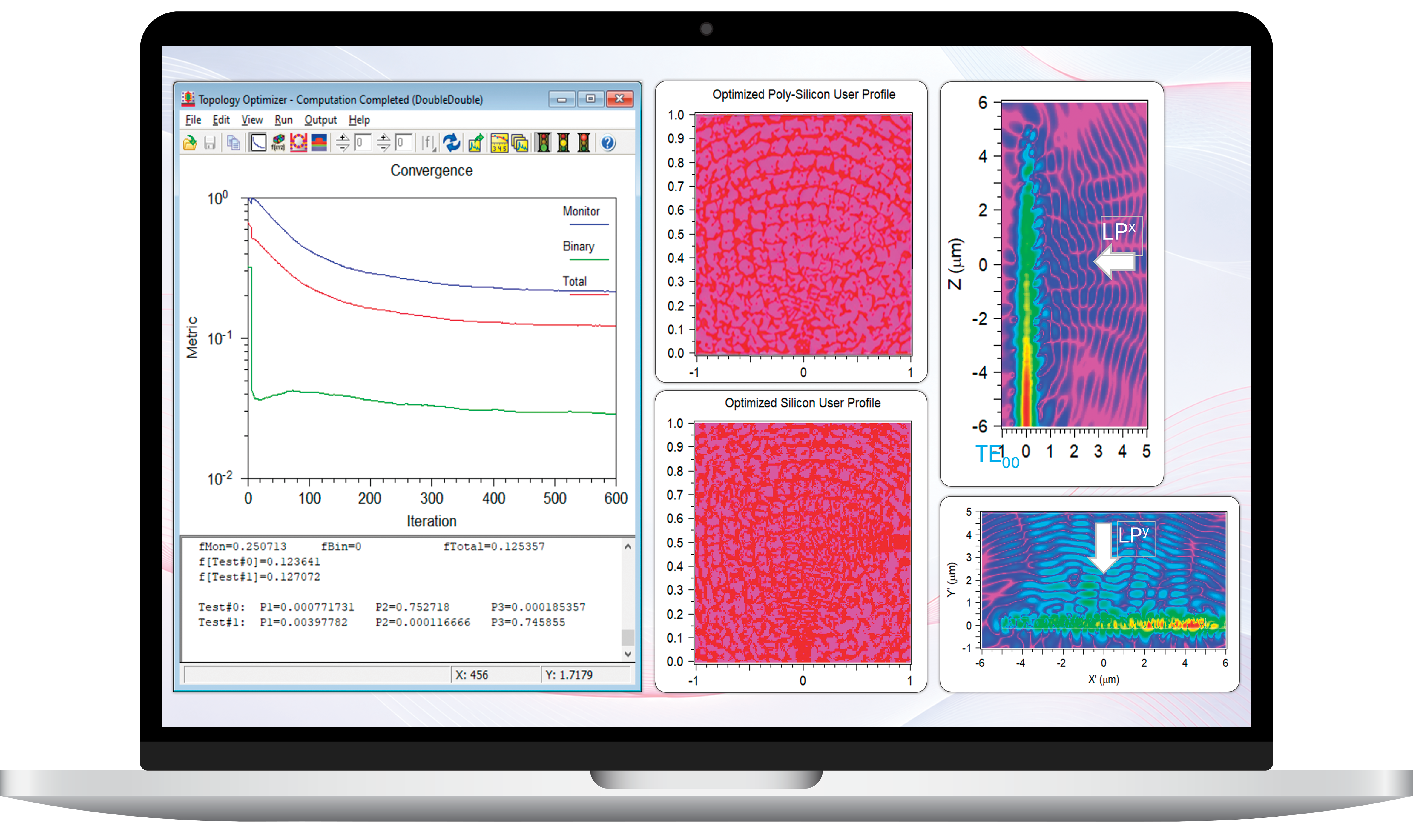
Connect electro-optical system design with physics-based component optimization.


- How to Analyze Signal Integrity Using Layout Geometry

- How to Design Soft-Switching Power Converter
- How to Optimize a PIN Photodetector Model for a Silicon Photonics Foundry Process

Learn from Industry Experts
Keysight 3D Interconnect Designer provides a physically aware environment for early exploration and validation of advanced interconnect architectures. The solution enables engineering teams to model and analyze complex 2.5D and 3D connectivity structures during the architecture phase, before committing to detailed physical implementation.

Blogs
Bootcamps
More Resources
白書
Mitigating Signal Integrity Challenges in High-Speed Chiplet Designs
ソリューション概要
3D Interconnect Designer: Physically Accurate Design and Exploration of Advanced 2.5D and 3D Interconnects
アプリケーションノート
End-to-End Electrical-Optical-Electrical Flow in Keysight ADS
白書
Choosing the Right Photonic Device Design Software
eBooks
Simulating & Optimizing RF Circuits in 3DHI Advanced Packaging
RTL and Packaging Design FAQs
Keysight provides an integrated design environment for RF ICs, chiplets, 3DICs, and advanced packages. Engineers can model, simulate, and verify electrical, electromagnetic, thermal, and interconnect performance throughout the design flow, helping reduce risk and accelerate development.
Chiplet-based architectures increase interconnect complexity and require accurate analysis of die-to-die channels, interposers, bridges, power delivery networks, and package effects. Early modeling and validation help optimize performance and avoid costly redesigns later in the development cycle.
Keysight Advanced Design System (ADS) combines circuit, electromagnetic, and system simulation in a single environment, enabling engineers to evaluate performance, optimize designs, and verify functionality across IC, package, and system domains.
As semiconductor devices become more complex, power efficiency is critical for performance, cost, and sustainability goals. Early power analysis helps teams identify inefficiencies, reduce power consumption, and improve overall design quality before implementation.
Electrical and thermal effects are closely linked in advanced ICs and packages. Electro-thermal simulation helps engineers predict temperature-related performance issues, evaluate reliability, and optimize designs before hardware is built.
Yes. By enabling early design exploration, integrated multi-physics analysis, and comprehensive verification across silicon, package, and interconnect technologies, Keysight EDA solutions help engineering teams reduce iterations, improve confidence, and shorten development cycles.