Choose a country or area to see content specific to your location
確認您的國家或地區
中國臺灣
請確認
Confirm your country to access relevant pricing, special offers, events, and contact information.
Pinpoint interference with post-processing spectrum management software in the lab.
Use this selector tool to quickly identify the best power supply for your aerospace and defense ATE requirements.
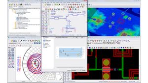
3D Interconnect Designer provides a flexible modeling and optimization environment for any advanced interconnect structure, including chiplets, stacked die, packages, and PCBs.
Get faster digital validation for less with a trade-in.
Emulate every part of your data center infrastructure. Emulate Anything. Optimize Everything.
With extra memory and storage, these enhanced NPBs run Keysight's AI security and performance monitoring software and AI stack.
Achieve fast, accurate board-level testing with robust inline and offline ICT designed for modern manufacturing.
Explore curated support plans, prioritized to keep you innovating at speed.
Authoritative application notes, data sheets, reference designs, and test procedures to accelerate design and validation decisions.
Hands‑on bootcamps that teach system design, test methods, and production workflows engineers can apply immediately.
Success Stories
全年無休的自助服務入口網站
更多的產品支援資訊
更多可協助您加速創新的是德科技服務
先進設計系統(ADS)的電路波封(CE)元件包含以下功能:
電路波封元件(Circuit Envelope Element)可為 Keysight EEsof EDA 的旗艦產品/高頻混合信號電子設計自動化(EDA)領域的技術創新領導者:先進設計系統(ADS),提供調變與暫態射頻模擬功能。ADS 提供獨家的設計模擬平台,可支援高頻和高速應用中的 IC、封裝和電路板協同設計。它完美地整合系統、電路、全 3D 電磁模擬與是德科技測試儀器,讓您能夠反覆執行一次到位的電子設計流程。 電路波封高效模擬在調變和暫態射頻激發驅動下的電路和系統。創新模擬科技克服了諧波平衡的記憶體限制,及暫態模擬器的時間成本,電路波封對非線性設計特別好用,能滿足 3G 和 4G 無線標準如 LTE 和 WiMax™。這個情況下,比起使用諧波平衡模擬中的功能如穩態激發,電路波封包含真實的調變與暫態射頻載波信號,能準確地模擬無線規格如誤差向量振幅(EVM)、相鄰通道功率比(ACPR)和誤碼率(BER)。 其他波封模擬器只能使用系統行為模式,並只能模擬射頻波封的載波,且不考慮阻抗不匹配,而電路波封並沒有這些限制。它允許任意電路、系統、和量測 X 參數區塊的組合,來準確地模擬調變射頻信號,並可考慮整個網路上的信號反射和混頻效應。 電路波封使用所有 X 參數的優勢,是德科技的最新創新,能從非線性向量網路分析儀(NVNA)量測結果擷取完整的非線性特性。讓您利用現成的元件測得的 X 參數,在數位調變射頻激發下進行準確的非線性設計,如功率放大器線性度和附加功率效率(PAE)最佳化,這是其他波封模擬器做不到的! ADS 電路波封元件需要 ADS 諧波平衡元件的功能才能運作。