
M8135A & M8136A Universal Signal Processor Architecture (USPA)
資料表
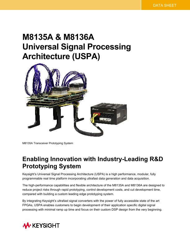
Enabling Innovation with Industry-Leading R&D Prototyping System
Keysight’s Universal Signal Processing Architecture (USPA) is a high performance, modular, fully programmable real time platform incorporating ultrafast data generation and data acquisition.
The high-performance capabilities and flexible architecture of the M8135A and M8136A are designed to reduce project risks through rapid prototyping, control development costs, and cut development time, compared with building a custom leading edge prototyping system.
By integrating Keysight’s ultrafast signal converters with the power of fully accessible state of the art FPGAs, USPA enables customers to begin development of their application specific digital signal processing with minimal ramp up time and focus on their custom DSP design from the very beginning.
Application Flexibility
The M8135A preconfigured system is designed for single channel transceiver applications, while the M8136A offers maximum configuration flexibility to address a wide range of potential applications (e.g. multi-channel configurations) that the customer can develop on the USPA system. Potential applications:
• ASIC & Systems-On-Chip (SoC) Prototyping
• Coherent & Direct Detect Research and Development
• Ultra Fast Data Acquisition/Generation
• Optical Communications
• Wireless applications, 6G
• Radar
• Physics research
Maximum Capability for Today and Tomorrow
Investment in Keysight USPA modules and components can be staged, starting with a base configuration and scaling to match development needs. The modular architecture is reusable for future projects and is reconfigurable to support parallel projects.
System Overview
Hardware
The M8135A is a preconfigured system designed for typical Transceiver Prototyping, while the M8136A is a fully configurable system.
In general, the M8136A system consists of one or several proFPGA motherboards mounted with FPGA boards. The proFPGA motherboards provide the necessary infrastructure (power connector, Ethernet, debugging interfaces, reference clock and synchronization signals…) for the FPGA board. Three different FPGA board options (described in proFPGA FPGA Boards below) are available to meet basic to complex application needs. Up to 16 FPGA’s can be cascaded as needed to provide the required hardware resources to meet the highest complexity designs.
Keysight USP-DAC and USP-ADC Extension Boards (with respective data converters) are mounted on a XCVU9P FPGA board. A USP-DAC board connects the TX side of 48 of the FPGA’s GTY transceivers to the digital inputs of the DAC3 module. The USP-ADC board connects the digital outputs of the ADC3 module to the RX side of 48 GTY transceivers. The Extension Boards also provide all required power converters, low-speed adjustment ICs, and a microcontroller to optimize the performance of the DAC3 or ADC3 converter modules at the different sample rates.
The data converters in USPA are in the same family as those used in Keysight instruments and offer the same high reliability and quality.
The full rate digital data can be transferred via cable assemblies between the FPGA’s. Two cabling system options are available:
A) V2-cables: Proprietary, highest performance & best usability
B) QSFP28 cables: Industry standard