











- Überblick
- Alle Modelle
- Unterstützung
Gezielte elektromagnetische Fehler einbringen, um Schwachstellen aufzudecken
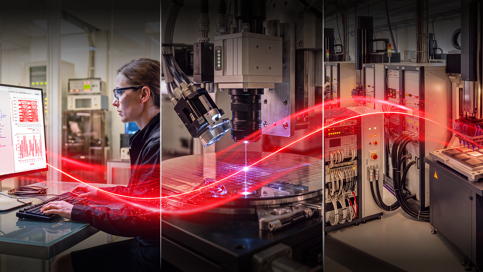
Elektromagnetische Fehlerinjektion (EMFI) ermöglicht es Sicherheitsexperten, mithilfe präzise erzeugter elektromagnetischer Impulse kontrollierte Fehler in ein Zielgerät einzuschleusen. Durch die Fokussierung elektromagnetischer Energie auf bestimmte Bereiche eines Chips können Prüfer das Geräteverhalten während sicherheitskritischer Vorgänge beeinflussen. Dies hilft, Schwachstellen aufzudecken, Gegenmaßnahmen zu bewerten und die Widerstandsfähigkeit eines Geräts gegen Fehlerangriffe zu validieren.
Lokalisierte Fehler einbringen
Test verpackter Geräte
Fehlereinspritzungsanalysen können ohne Chip-Depackaging durchgeführt werden, wodurch die Vorbereitungszeit verkürzt und die Zielbauteile geschont werden.
Optische Gegenmaßnahmen umgehen
Automatisierte und wiederholte Auswertungen

-
Maximum voltage
100 V ± 10% bis 475 V ± 10%
-
Maximum frequency
1 MHz
-
Product type
Bidirectional fault injection probe, Unidirectional fault injection probe
-
Technology
Device Security
Beliebteste Konfigurationen
Bidirektionale Fehlerinjektionssonde
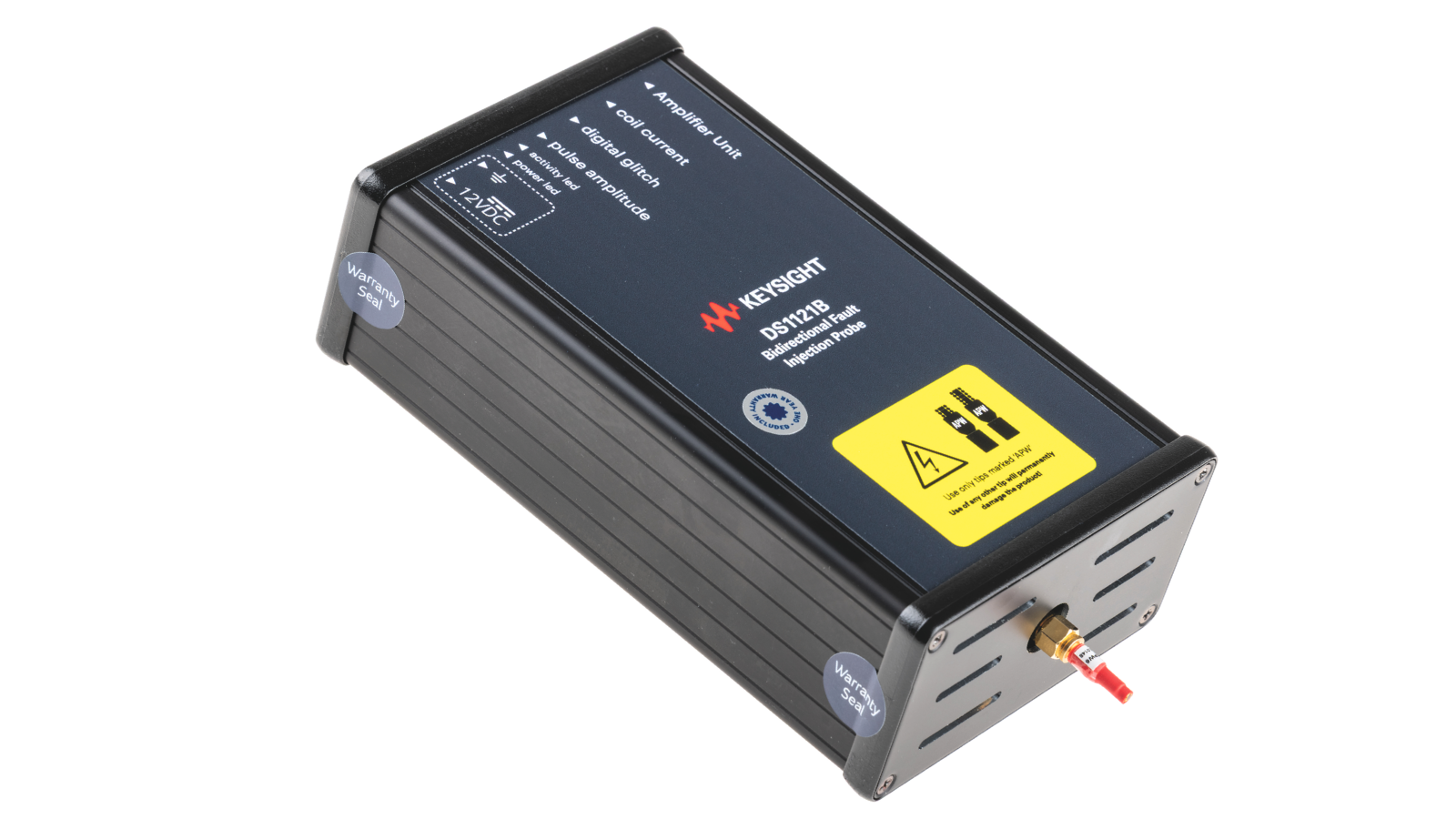
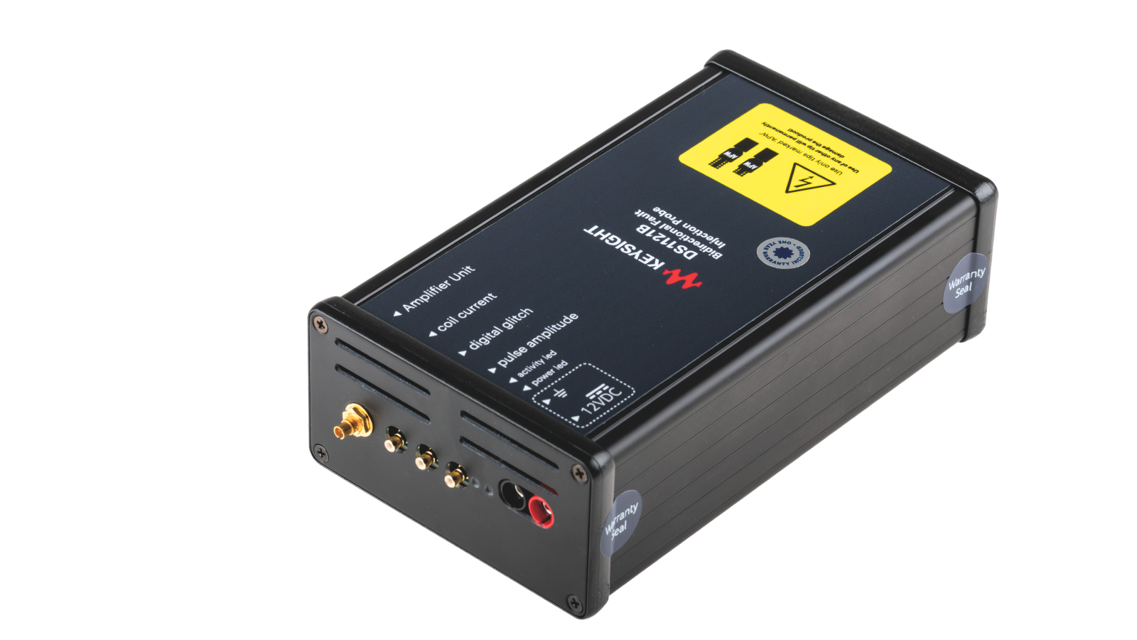
Die bidirektionale Fehlerinjektionssonde DS1121B erzeugt elektromagnetische (EM) Hochleistungsimpulse an präzisen, vom Benutzer definierten Stellen eines Zielgeräts. Ihre schnelle Impulserzeugung erfüllt die strengen Anforderungen sowohl kommerzieller als auch zertifizierter Prüfumgebungen.
Die bidirektionale Fehlerinjektionssonde DS1121B erzeugt elektromagnetische (EM) Hochleistungsimpulse an präzisen, vom Benutzer definierten Stellen eines Zielgeräts. Ihre schnelle Impulserzeugung erfüllt die strengen Anforderungen sowohl kommerzieller als auch zertifizierter Prüfumgebungen.

Unidirektionale Fehlereinspritzsonde
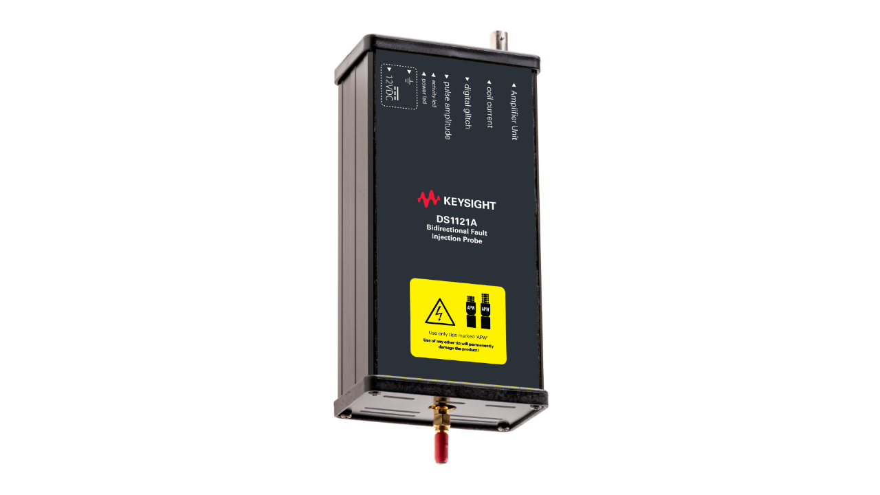
Die unidirektionale Fehlerinjektionssonde DS1120A erzeugt lokalisierte Fehler auf modernen Chips mithilfe schneller, vorhersagbarer und leistungsstarker elektromagnetischer Impulse.
Die unidirektionale Fehlerinjektionssonde DS1120A erzeugt lokalisierte Fehler auf modernen Chips mithilfe schneller, vorhersagbarer und leistungsstarker elektromagnetischer Impulse.
Bidirektionale Fehlerinjektionssonde
Induzieren von elektromagnetischen Impulsen zur Erzeugung lokaler Fehler auf modernen Chips.
Induzieren von elektromagnetischen Impulsen zur Erzeugung lokaler Fehler auf modernen Chips.
Dienstleistungen und Support
Innovieren Sie im Handumdrehen mit maßgeschneiderten Supportplänen und priorisierten Reaktions- und Bearbeitungszeiten.
Profitieren Sie von planbaren, leasingbasierten Abonnements und umfassenden Lifecycle-Management-Lösungen – damit Sie Ihre Geschäftsziele schneller erreichen.
Als KeysightCare-Abonnent profitieren Sie von einem erweiterten Service mit zuverlässiger technischer Unterstützung und vielem mehr.
Stellen Sie sicher, dass Ihr Testsystem den Spezifikationen entspricht und sowohl lokale als auch globale Standards erfüllt.
Schnelle Messungen dank hauseigener, von Ausbildern geleiteter Schulungen und E-Learning.
Laden Sie die Keysight-Software herunter oder aktualisieren Sie Ihre Software auf die neueste Version.
Häufig gestellte Fragen
Elektromagnetische Fehlerinjektion (EMFI) ist eine Hardware-Sicherheitstestmethode, die kurze, kontrollierte elektromagnetische Impulse nutzt, um den Betrieb eines Halbleiterbauelements vorübergehend zu stören. Durch die gezielte Zufuhr von Energie in bestimmte Bereiche eines Chips zu präzise gesteuerten Zeitpunkten können Sicherheitsexperten Fehler hervorrufen und beobachten, wie das Bauelement auf anormale Bedingungen reagiert.
EMFI funktioniert durch die Erzeugung eines schnellen elektromagnetischen Impulses mittels einer speziellen Sonde, die über dem Zielgerät positioniert ist. Der Impuls erzeugt eine lokale Störung im Chip, die potenziell das Verhalten von Schaltungen, das Timing, Speicheroperationen oder kryptografische Berechnungen beeinflussen kann.
Durch die Kontrolle von Impulszeitpunkt, -stärke und -ort können Ingenieure untersuchen, wie sich das Gerät unter Fehlerbedingungen verhält und potenzielle Sicherheitslücken identifizieren.
Beide Techniken zielen darauf ab, Fehler hervorzurufen, aber sie zielen auf unterschiedliche Weise auf das Gerät ab.
- Spannungsschwankungen führen zu Fehlern in der Stromversorgung des Geräts.
- EMFI injiziert Energie direkt in lokalisierte Bereiche des Geräts mittels elektromagnetischer Impulse.
Da EMFI gezielt bestimmte Bereiche eines Chips untersuchen kann, ohne die Stromversorgung zu verändern, bietet es oft eine größere Flexibilität bei der Bewertung komplexer oder hochintegrierter Bauelemente.
Bei der Laserfehlerinjektion wird fokussiertes Licht eingesetzt, um gezielt bestimmte Bereiche des Siliziumchips zu bearbeiten, was häufig einen physischen Zugriff auf den Chip erfordert. EMFI hingegen nutzt elektromagnetische Impulse und kann oft direkt an verpackten Bauteilen ohne Chipvorbereitung durchgeführt werden.
Dies macht EMFI zu einer attraktiven Option für viele Sicherheitsbewertungen, bei denen der Erhalt des Zielgeräts wichtig ist.
In vielen Fällen nein. Einer der Hauptvorteile von EMFI besteht darin, dass Tests oft direkt an verpackten Geräten durchgeführt werden können, ohne den Siliziumchip freizulegen. Dies reduziert die Vorbereitungszeit und ermöglicht es Ingenieuren, Produkte in einem Zustand zu bewerten, der ihrem Einsatzzustand sehr nahe kommt.
Unterschiedliche Sondenkonstruktionen erzeugen unterschiedliche elektromagnetische Feldcharakteristika und Angriffsprofile.
Je nach Evaluierungsziel können Ingenieure eine unidirektionale oder bidirektionale Sonde wählen, um die Zielgenauigkeit, die Fehlererzeugung und die Angriffsabdeckung zu optimieren. Die geeignetste Option hängt vom zu testenden Gerät und der Art der durchgeführten Fehlereinspeisungskampagne ab.
Ja. EMFI-Systeme lassen sich mit Positionierungssystemen und der Inspector-Software kombinieren, um Scans, Fehlerinjektionskampagnen, Parameter-Sweeps und die Ergebnisanalyse zu automatisieren. Die Automatisierung trägt zur Verbesserung der Reproduzierbarkeit und zur Beschleunigung der Schwachstellenerkennung bei.
EMFI ist im Allgemeinen darauf ausgelegt, temporäre und kontrollierte Fehler zu erzeugen, anstatt das Gerät dauerhaft zu beschädigen. Wie bei jeder Fehlereinspeisungsmethode sollten die Tests jedoch unter geeigneten Betriebsbedingungen und gemäß den entsprechenden Auswertungsverfahren durchgeführt werden.
Ja. Die Inspector-Software unterstützt automatisierte Workflows für die Fehlereinspeisung, die Verwaltung von Angriffskampagnen, Parameteranalysen und die Auswertung von Ergebnissen. In Kombination mit Positionierungssystemen und Fehlereinspeisungssonden trägt sie dazu bei, effiziente und reproduzierbare EMFI-Evaluierungen zu erstellen.
Ja, es verringert das Risiko einer dauerhaften Beschädigung des Geräts im Vergleich zu laserbasierten Verfahren, da das Silizium nicht direkt mit konzentrierter optischer Energie abgetragen oder erhitzt wird.
In der Regel muss man den genauen Ort nicht im Voraus kennen. Ein gängiger Arbeitsablauf sieht vor, dass eine größere Spule die Chipoberfläche breitflächig abtastet (oft kombiniert mit einer automatisierten XYZ-Tischabtastung), um empfindliche Bereiche zu identifizieren. Anschließend wird auf eine kleinere, fokussiertere Spule umgeschaltet, um den Fehler an dieser präzisen Stelle zu verfeinern und zu wiederholen.