Choose a country or area to see content specific to your location
O que você está procurando?
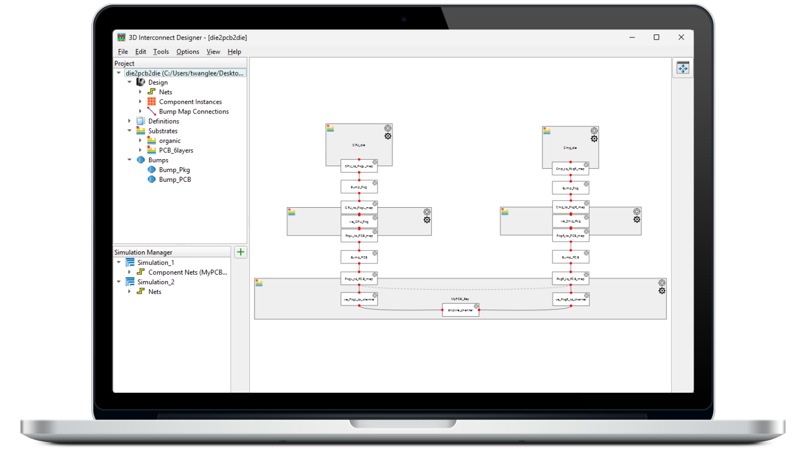
Design, model, and validate complex 3D interconnect architectures with a powerful standalone design environment.
Automate transmitter and receiver validation across next-generation I/O, memory, and fabric interfaces.
Strengthen 1.6T network reliability for AI-scale workloads from transceivers to interconnects.

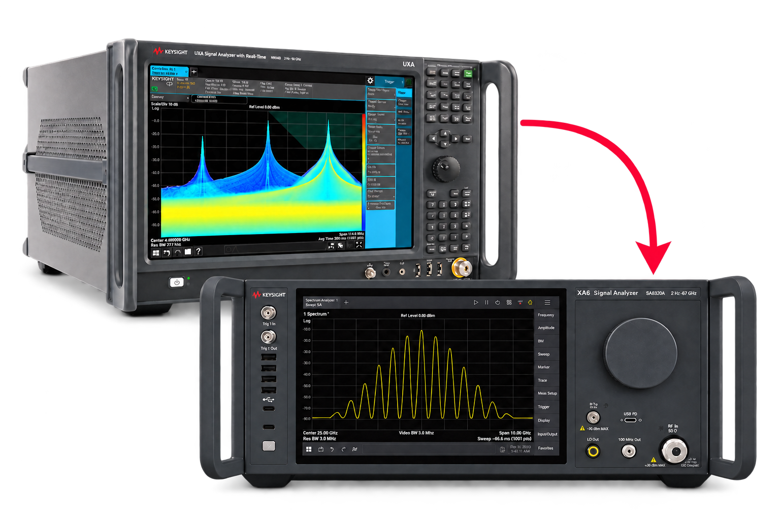
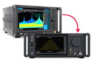
Pair Keysight VSA software with the new XA5 signal analyzer for advanced visualization, demodulation, and analysis — start your 30-day trial today.
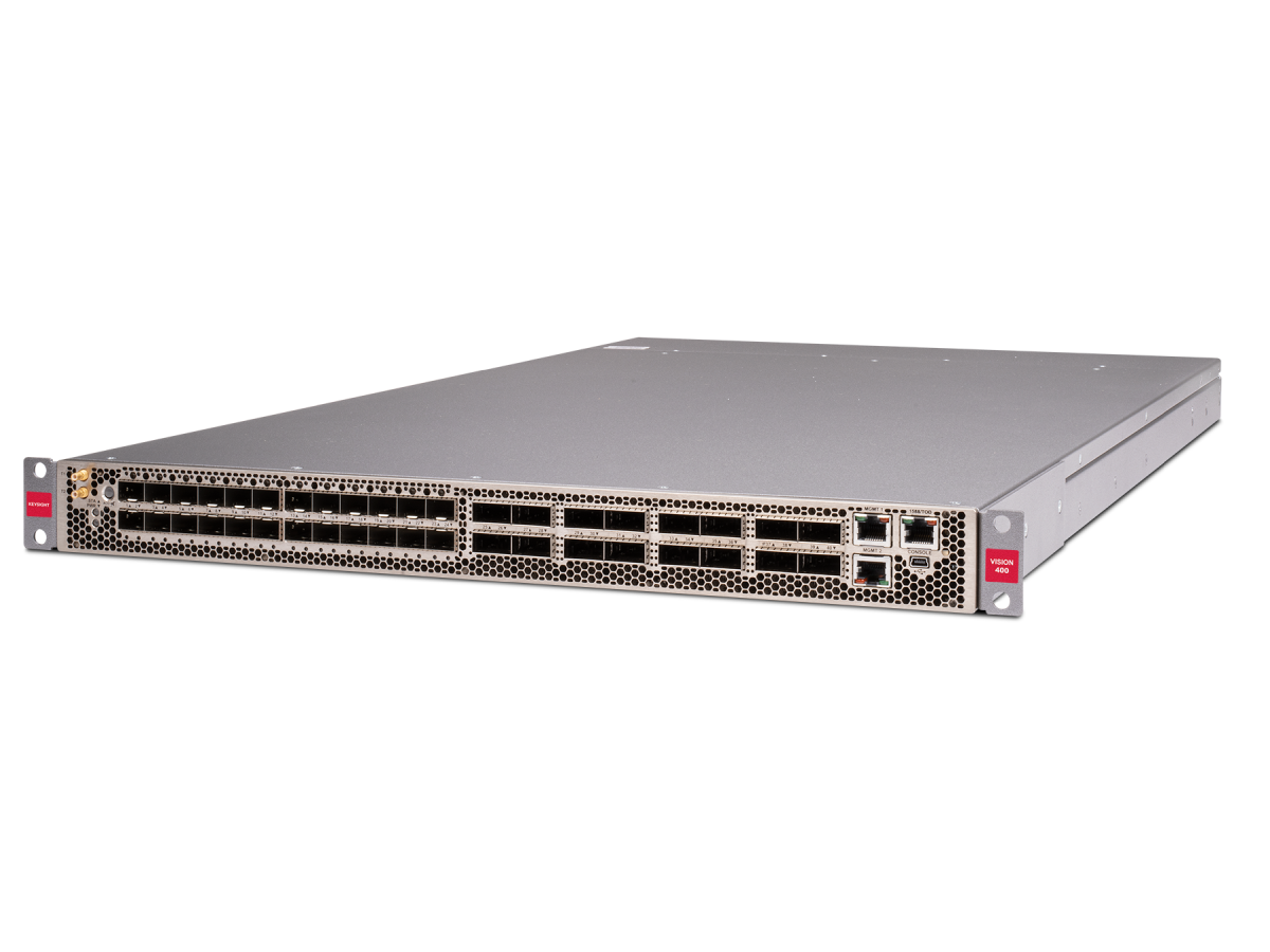
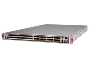
With extra memory and storage, these enhanced NPBs run Keysight's AI security and performance monitoring software and AI stack.
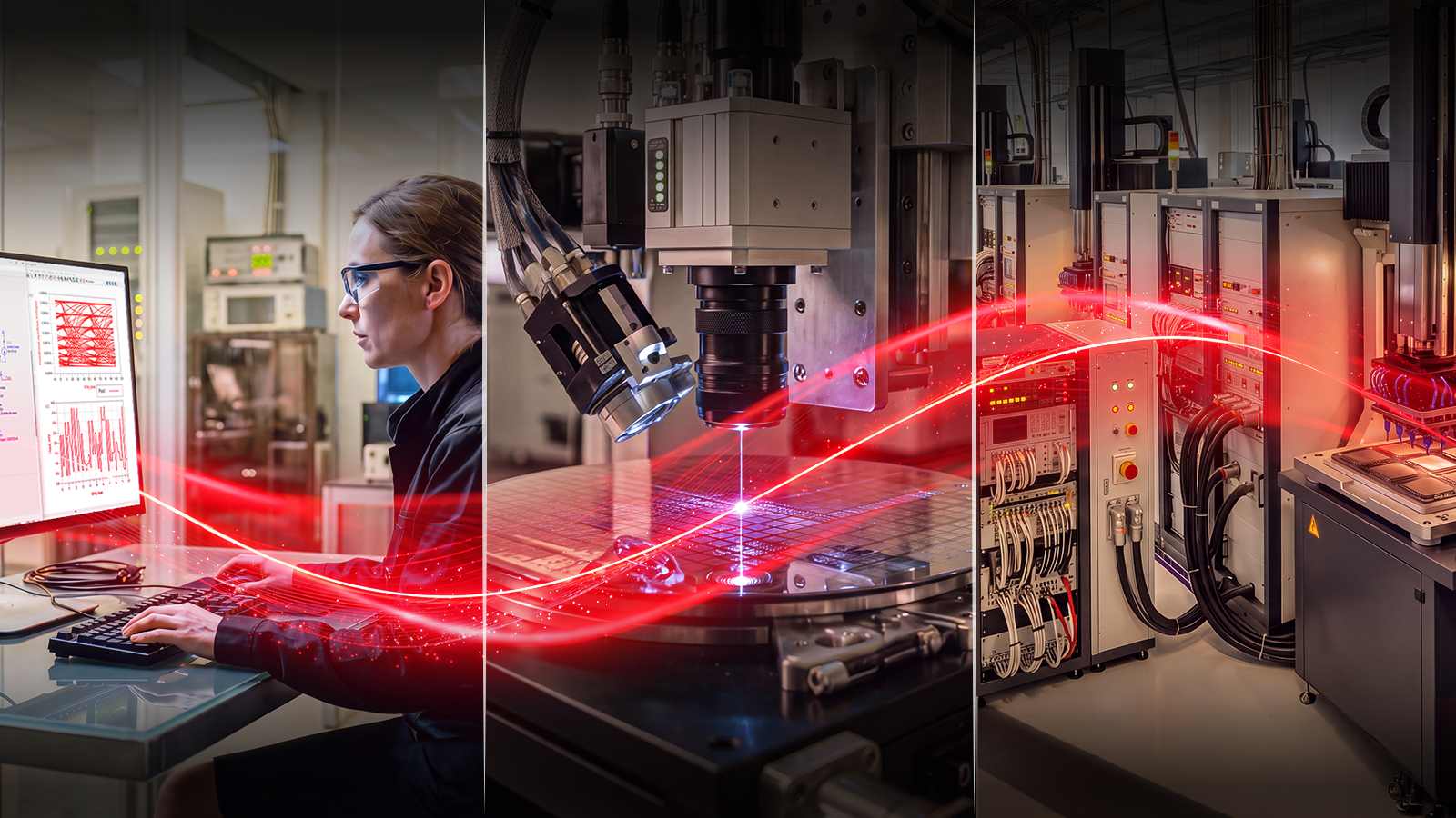
Explore end-to-end workflows spanning IC design, validation, wafer test, and photonics.

Explore curated support plans, prioritized to keep you innovating at speed.
Maximize accuracy and performance with precision accessories engineered for Keysight instruments.
Save up to 50% on our latest instruments with eligible Keysight or competitor trade-ins.
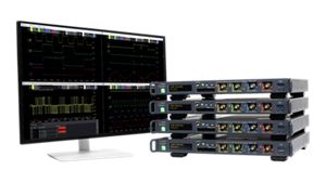
Four channels per 1U of rack space, up to 1 GHz bandwidth, and multi-oscilloscope synchronization.
Purpose-built solutions engineered for the design and test challenges unique to your industry.
Use Cases mapped to every stage of your product lifecycle, from design through operations.
Success Stories
Authoritative application notes, data sheets, reference designs, and test procedures to accelerate design and validation decisions.
Hands‑on bootcamps that teach system design, test methods, and production workflows engineers can apply immediately.
Learning Hub
Explore methodologies, test strategies, and technical resources for designing, validating, and scaling AI systems and networks.
Quick access to the most frequent support related self-help tasks.
Additional content to support your product needs.
Explore services to accelerate every step of your innovation journey.
Accelerate innovation across ICs, chiplets, packages, boards, optics, and system architectures powering next-generation AI and hyperscale data centers.
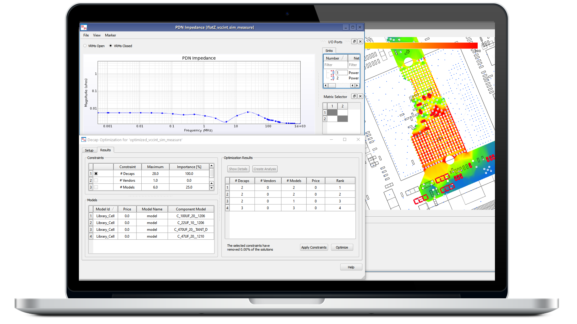
Analyze IR drop, ground bounce, electromagnetic interference, and power distribution behavior to ensure stable operation of AI accelerators, processors, and high-density server platforms.
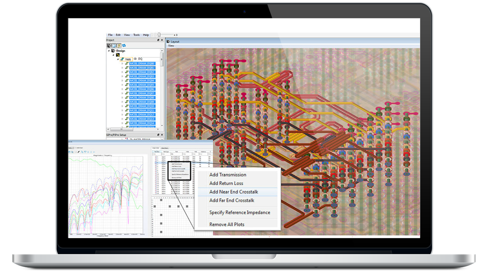
Identify channel losses, crosstalk, reflections, and impedance discontinuities affecting multi-gigabit chiplet interconnects and advanced package communication pathways.
Perform electro-thermal co-simulation to predict hotspots, thermal coupling, and temperature-driven performance degradation in high-power data center devices.
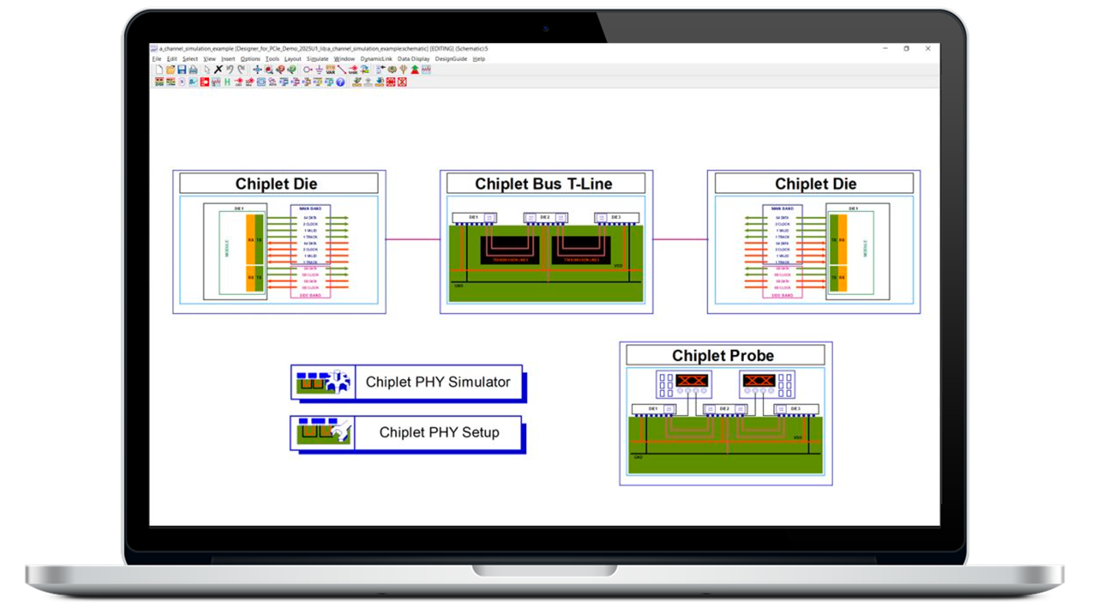
Design and validate UCIe and BoW interfaces, ensuring interoperability, signal integrity, and reliable communication between chiplets in heterogeneous systems.
Create physically accurate models spanning chip, package, board, and system domains to analyze performance across the complete signal path.
Evaluate stacked die architectures, interposers, and advanced packaging technologies to improve performance, bandwidth density, and integration efficiency.
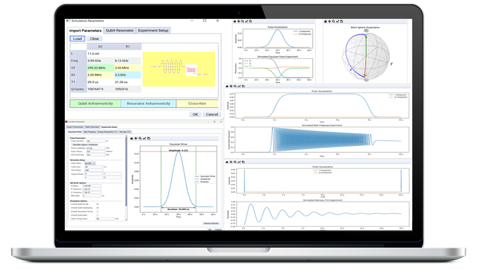
Design quantum devices, qubit control electronics, amplifiers, interconnects, and system architectures supporting scalable quantum computing infrastructure.
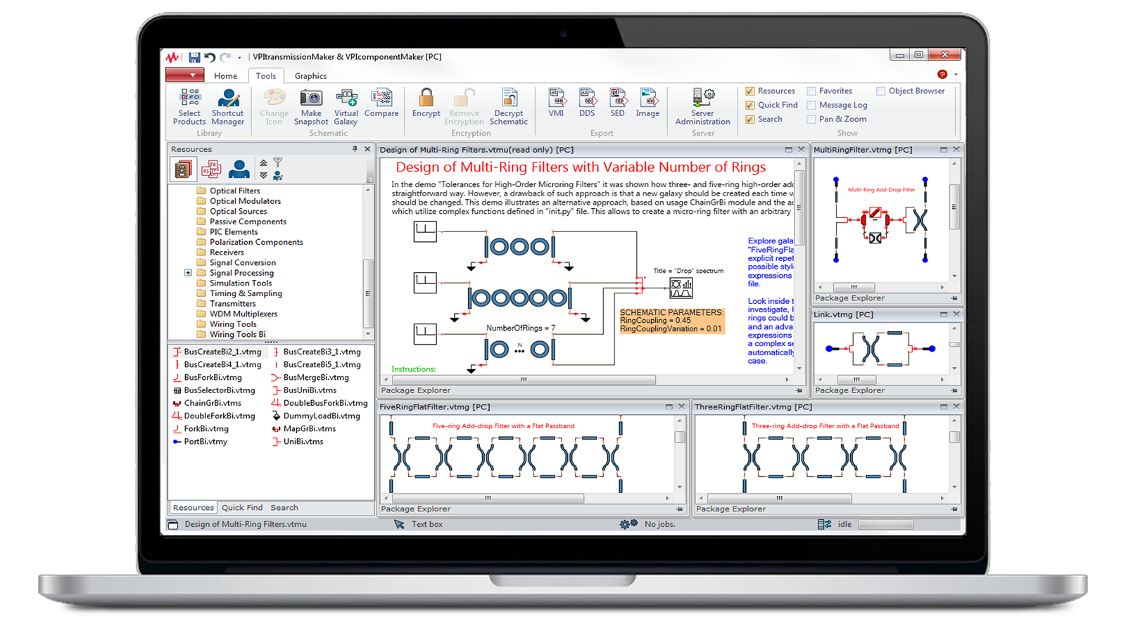
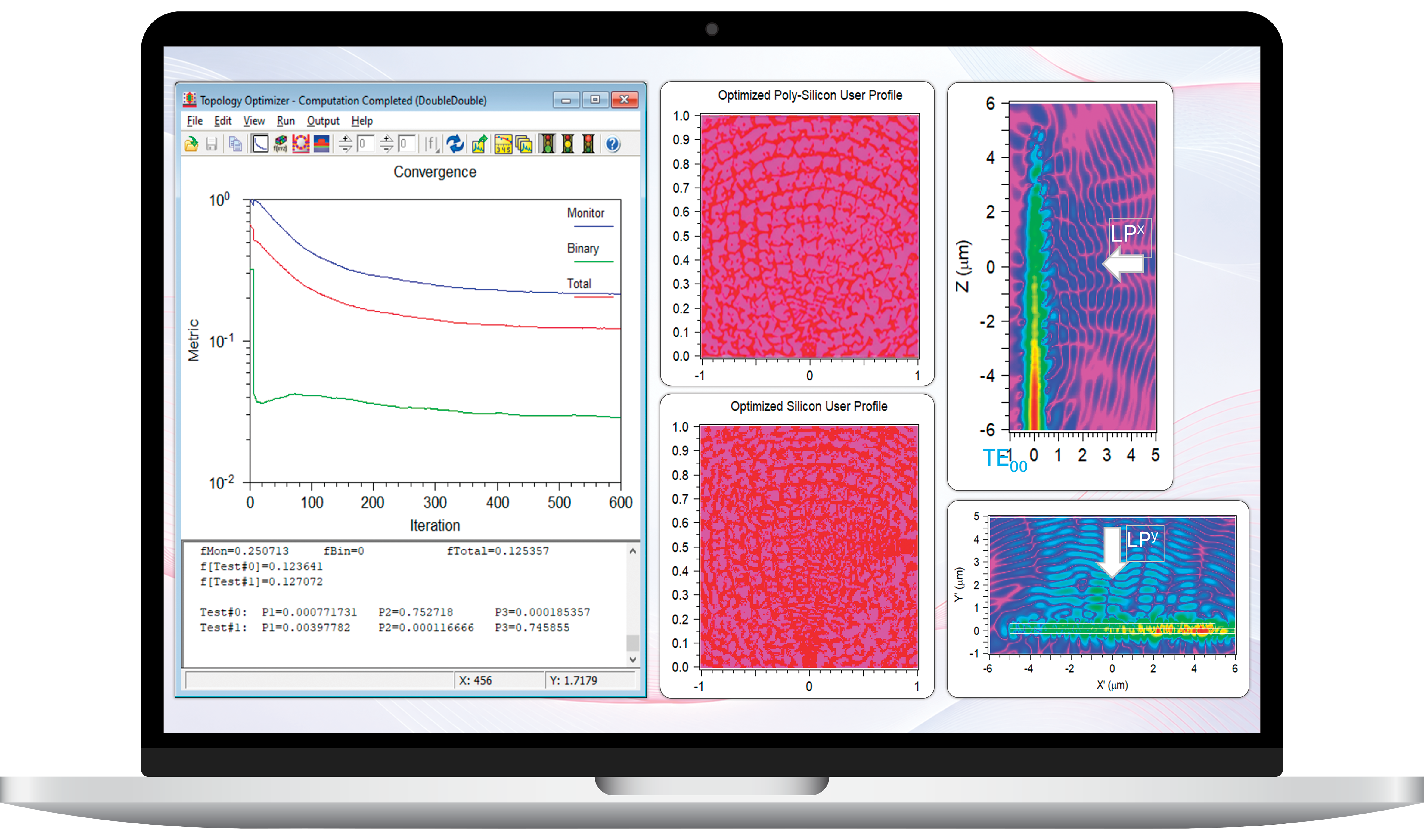
Design and simulate photonic integrated circuits for optical communication, high-bandwidth interconnects, and emerging data center technologies.
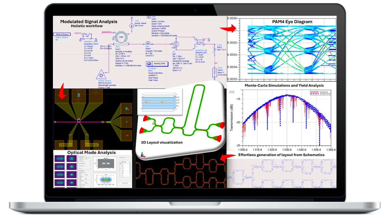
Bridge photonic device behavior with circuit and system performance to accelerate development of optical networking and compute architectures.
Simulate complete electrical-optical-electrical signal chains to optimize high-speed Ethernet modules, transceivers, and optical communication interfaces.
Design co-packaged optical solutions that reduce power consumption and bandwidth bottlenecks in next-generation AI and cloud computing platforms.
Model optical transmission systems and network architectures connecting hyperscale facilities while optimizing capacity, reach, latency, and signal quality.
Case Studies
Case Studies
Case Studies
Case Studies
Case Studies
Case Studies
Case Studies
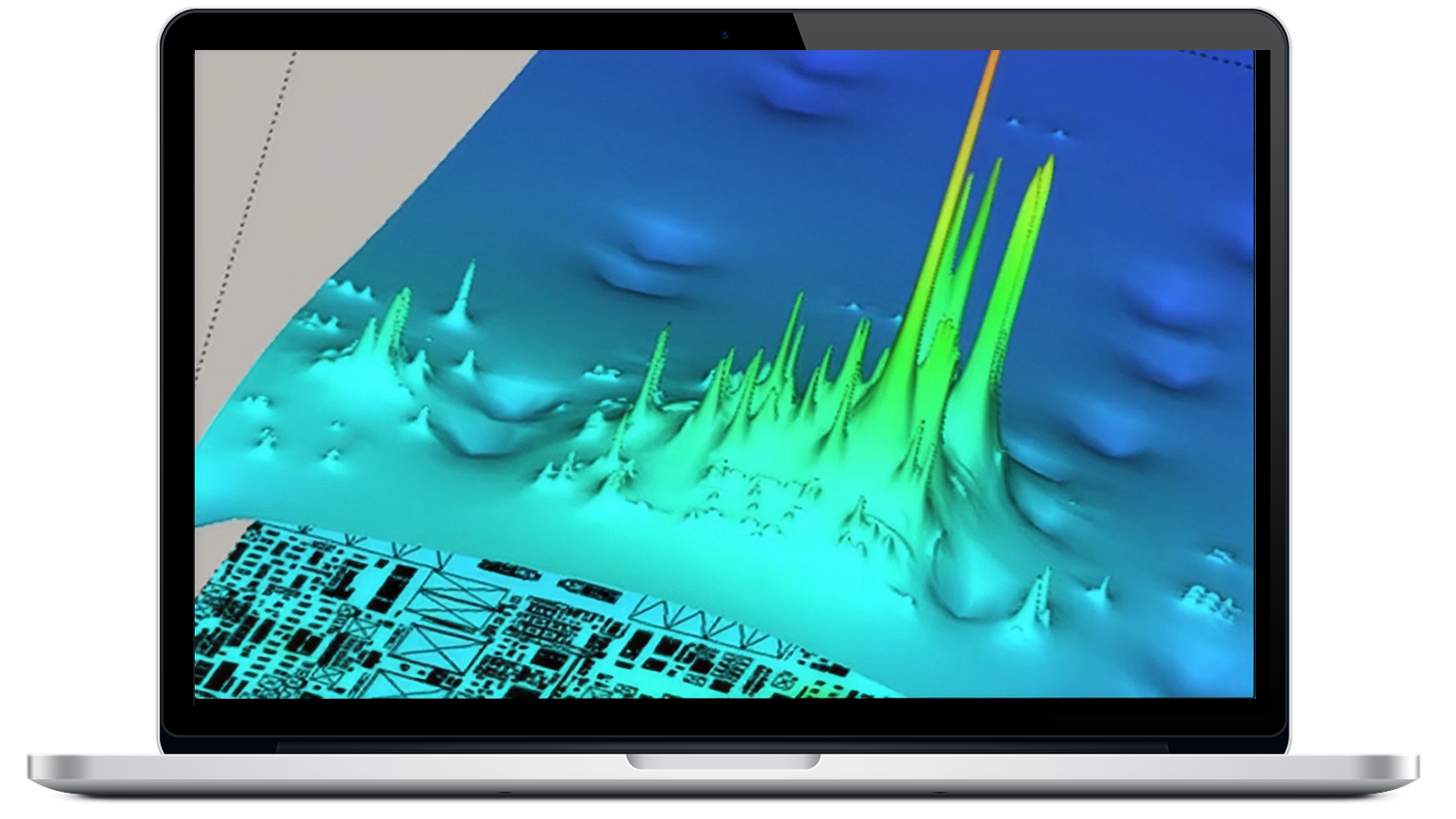
Accurate simulation prediction and mitigation requires full 3D EM simulation of the PCB power delivery network (PDN), end-to-end voltage regulator module (VRM) + PCB PDN, and dynamic load digital twin modeling. Other considerations include harmonic balance analysis for steady state transient nonlinear behavior, and careful separation of crosstalk and ground bounce noise sources. By integrating these techniques into the design process, engineers can significantly reduce the risk of late-stage failures, improve system reliability, and meet the stringent design requirements for designing AI, cloud computing, and advanced semiconductor architectures.
blogs
blogs
blogs
blogs
This EDA bootcamp begins with foundational concepts and analysis techniques, then progresses through simulation, design strategies, and advanced troubleshooting methods using real-world tools and examples.
Power Integrity experts explore Power Delivery Networks topics and approaches to avoid design pitfalls using Keysight ADS with the Power Integrity bundle.
Dive deeper into designing with Signal Integrity with EDA. This boot camp provides a solid foundation in Signal Integrity concepts. Keysight technical experts apply these concepts to current digital standards covering USB, PCIE and Chiplets.
This bootcamp guides you through the design of superconducting qubits, quantum amplifiers and systems.
Learn the basics of designing with Chiplets, a promising alternative to monolithic System-on-Chips (SoCs). Chiplets are also a key enabler of heterogeneous and modular SoC design, which can accelerate innovation and adaptation in the electronic industry.
This bootcamp demonstrates how to overcome the challenges of designing 3DHI RF Modules. Keysight ADS with RFPro provides the only fully integrated environment for RF 3DHI module and RF chiplet design, simulation, and optimization in complex systems.
eBooks
White Papers
Notas de Aplicação
WEBINARS
White Papers
Notas de Aplicação
Notas de Aplicação
EDA software enables engineers to predict power, thermal, signal integrity, and system behavior before fabrication, reducing development risk and accelerating deployment.
Simulation tools optimize power delivery networks, package architectures, thermal performance, and high-speed interconnects required for modern AI workloads.
Power integrity analysis helps identify IR drop, voltage fluctuations, ground bounce, and EMI issues that affect reliability and performance.
As data rates increase, channel losses, crosstalk, reflections, and impedance discontinuities can significantly degrade system performance and reliability.
Chiplets improve scalability, yield, and performance by enabling heterogeneous integration while reducing development costs and accelerating innovation.
Electro-thermal simulation predicts how temperature impacts electrical performance, helping engineers mitigate hotspots and improve reliability.
Co-packaged optics shortens electrical interconnect distances, reduces power consumption, and enables higher bandwidth densities for AI and cloud systems.
Photonic technologies provide scalable bandwidth, lower latency, and improved power efficiency to support rapidly growing network traffic demands.
Yes. Full-stack simulation environments enable engineers to analyze interactions across dies, packages, PCBs, optics, and system-level architectures.
By enabling virtual prototyping, early verification, and cross-domain optimization, EDA tools help teams deliver advanced computing and networking technologies faster and with greater confidence.
Talk to our team to find the right solution for your design needs, get a personalized quote, or request a free trial.
O que você está procurando?