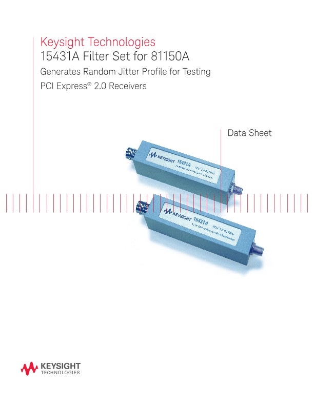
15431A Filter Set for 81150A
資料表
PCI Express 2.0 Physical Layer Testing
Increasing speed rate for PCI Express Generation 2 is driving design to new dimensions. Validating and testing of PCI Express devices at the physical layer is getting more and more challenging for today’s engineers.
PCIe ® 2.0 doubles the data rate from 2.5 Gbit/s to 5 GBit/s, improves point-to-point data transfer protocol and becomes more tolerant of jitter. Therefore the jitter tolerance and transfer measurement become more important.
Keysight’s Offering
Keysight Technologies, Inc. offers serial and multi-lane RX testing.
J-BERT N4903A High-Performance Serial BERT
allows single-lane characterization of jitter tolerance from the device’s input, checks compliance by emulating jitter conditions and has built-in mask tests and eye analysis tools to evaluate the PCIe 2.0 design.
ParBERT 81250A High-Performance Parallel Bit Error Ratio Tester is a modular BERT platform for clock, data generation and data analysis that allows configuring of a solution with up to 64 output and input channels. Its jitter modulation capability via the delay control input, together with the PCIe multi-lane receiver compliance test suite make it an automated and highly accurate tool for multi-lane PCI Express receiver tolerance compliance and characterization testing. The PCIe 2.0 specification defines a dedicated random jitter profile. The required control voltage for ParBERT’s delay control input can be generated by the Keysight 81150A, a pulse function arbitrary noise generator.
The 81150A Pulse Function Arbitrary Noise Generator
provides white Gaussian noise with a selectable crest factor up to 7 (Vpeak / VRMS) or 14 (Vpeak peak / VRMS). The long repetition rate of 26 days ensures real random noise. After 26 days the noise pattern starts from the beginning.
The Keysight 15431A noise filter is an instrument accessory that is intended to be used for jitter measurements on PCIe 2.0 with the 81150A as noise source and the N4903A or the 81250A as jitter tolerance tester.The proper jitter spectrum is achieved by filtering the white noise with a PCIe 2.0-specific filter. The filter can serve two topologies: data driven and common clock.
Test Setup of a J-BERT
Test setup of a J-BERT with the 81150A for LF noise; the filtered signal from the 81150A is used as delay control input for the J-BERT.
An equivalent setup is valid for the ParBERT 81250A.
The N5990A test automation software supports PCIe 2.0 compliance testing and characterization with J-BERT and ParBERT configurations.
Setting the correct output amplitude on the 81150A
For the reference clock filter the total rms jitter is (4.2² + 3.4²)½ = 5.4 ps. The sensitivity of the J-BERT delay control input is specified with 400ps/V. Thus the filter’s output voltage must be 5.4/400 = 0.0135 VRMS or 13.5 mVRMS. With an insertion loss of 21.4 dB for the filter, the appropriate 81150A output voltage is 159 mVrms. The equivalent calculation for the data clocked filter with a total RMS jitter of 9 ps and 21.9 dB insertion loss yields 280 mVRMS.