Here's the page we think you wanted.
See search results instead:
Choose a country or area to see content specific to your location
What are you looking for?
Suggested searches
No product matches found - System Exception
Matched content
-
-
Integrated Physics Suite
Bridging design and physical testing to evaluate drop, impact, shock, and vibration compliance before hardware exists.


-
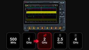
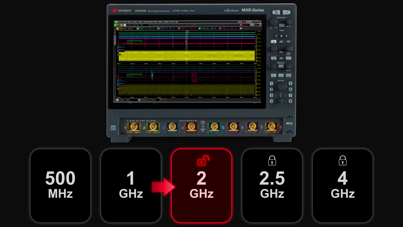
Buy an Expert Oscilloscope, Boost Your Bandwidth
Unlock your free upgrade to the next bandwidth tier.
-
End-to-End Validation for AI Data Center
Strengthen 1.6T network reliability for AI-scale workloads from transceivers to interconnects.

-
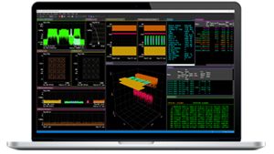
Take On Complex MIMO Signals
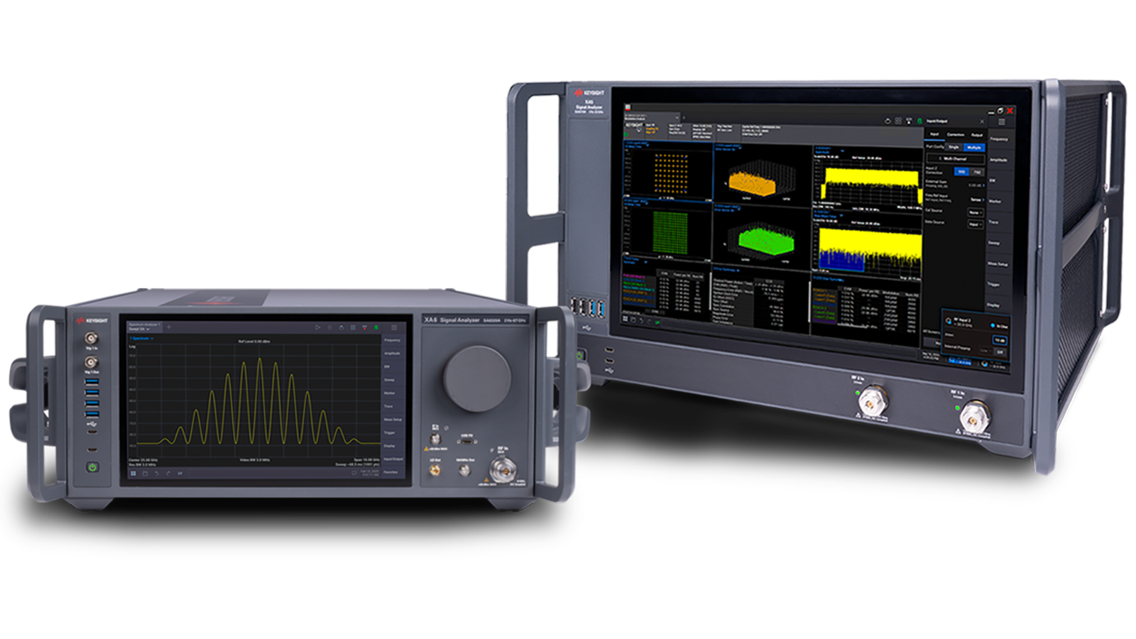
Pair Keysight VSA software with the new XA5 signal analyzer for advanced visualization, demodulation, and analysis — start your 30-day trial today.
-
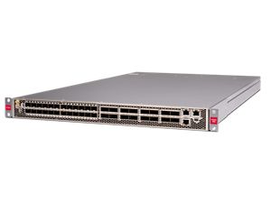
Introducing AI-Enhanced Packet Brokers
With extra memory and storage, these enhanced NPBs run Keysight's AI security and performance monitoring software and AI stack.
-
Accelerate Semiconductor Innovation
Explore end-to-end workflows spanning IC design, validation, wafer test, and photonics.

-
Accelerate Your Innovation Engine
Explore curated support plans, prioritized to keep you innovating at speed.

-
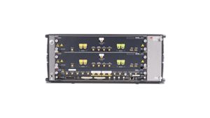
448 Gb/s Waveform Generation
Achieve 200+ Gbaud multi-level modulated signals with high-speed AWGs for digital and optical standards.
-
The Right Connection Makes the Measurement
Maximize accuracy and performance with precision accessories engineered for Keysight instruments.

Analyze Complex RF Signals FasterExplore dual-channel and ultra-wideband signal analysis for demanding RF workflows.
 Digital Validation. Faster.
Get faster, clearer insights with our new multicore, 12-bit oscilloscope up to 33 GHz. Trade in your old oscilloscope and get credit toward a new XR8.
-
-
Purpose-built solutions engineered for the design and test challenges unique to your industry.
Use Cases mapped to every stage of your product lifecycle, from design through operations.
Success Stories
HPE Juniper Networking Builds Next-Gen AI Infrastructure -
Authoritative application notes, data sheets, reference designs, and test procedures to accelerate design and validation decisions.
FeaturedHands‑on bootcamps that teach system design, test methods, and production workflows engineers can apply immediately.
Learning Hub
AI TechnologyExplore methodologies, test strategies, and technical resources for designing, validating, and scaling AI systems and networks.
- Buy
-
Quick access to support related self-help tasks.
Additional content to support your product needs.
Do more with Keysight ServicesExplore services to accelerate every step of your innovation journey.










Parametric Test Solutions Wafer-level test systems for parametric validation
Model: NX5402A
prev
- Overview
- Options
- Accessories
- Software
- Support
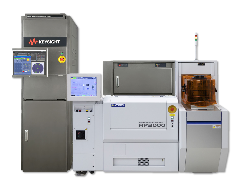
Silicon Photonics Wafer Test System
NX5402A Silicon Photonics Wafer Test System provides all required features for volume production testing such as WAT or PCM with a fully automated wafer prober.
-
Additional features
One-pass optical & electrical test
-
Maximum number of measurement pins
12 (optical in), 12 (optical out), 30 (electrical)
-
Minimum voltage measurement resolution
N/A
-
Minimum current measurement resolution
N/A
Ready for a quote
Find out what's included and explore available upgrade options from Keysight.
Highlights
- One-stop integrated solution with optical/electrical test capabilities for fully-automated wafer prober
- Automated one pass testing for complex and massive optical and electrical measurements
- Volume production-ready with SECS/GEM Factory Automation, safety interlock, and clean room-ready features
- High throughput testing by optimized fiber alignment and multi-channel optical/electrical test architecture
- Guaranteed system performance by Keysight's Advanced Wafer-Level Photonic Calibration
- Dedicated support model enabling high system availability for production
- Keysight-developed Fiber Alignment and Positioning System
- Leading-edge PathWave Semiconductor Test software integrating Keysight SPECS
- Reliable performance monitoring by Build-in Automatic System Diagnostics
- Automated Multi-Recipe Execution software enabling multiple recipes to run in batch mode
Services and support
Innovate at speed with curated support plans and prioritized response and turn-around times.
Get predictable, lease-based subscriptions and full lifecycle management solutions—so you reach your business goals faster.
Experience elevated service as a KeysightCare subscriber to get committed technical response and more.
Ensure your test system performs to specification and meets local and global standards.
Make measurements quickly with in-house, instructor-led training, and eLearning.
Download Keysight software or update your software to the newest version.
Start your quote by choosing a product
Select a configuration below