Choose a country or area to see content specific to your location
国の設定をご確認下さい。
ご確認ください
Confirm your country to access relevant pricing, special offers, events, and contact information.
Explore dual-channel and ultra-wideband signal analysis for demanding RF workflows.
Get faster, clearer insights with our new multicore, 12-bit oscilloscope up to 33 GHz. Trade in your old oscilloscope and get credit toward a new XR8.
Bridging design and physical testing to evaluate drop, impact, shock, and vibration compliance before hardware exists.
Unlock your free upgrade to the next bandwidth tier.
Strengthen 1.6T network reliability for AI-scale workloads from transceivers to interconnects.
Pair Keysight VSA software with the new XA5 signal analyzer for advanced visualization, demodulation, and analysis — start your 30-day trial today.
With extra memory and storage, these enhanced NPBs run Keysight's AI security and performance monitoring software and AI stack.
Explore end-to-end workflows spanning IC design, validation, wafer test, and photonics.
Explore curated support plans, prioritized to keep you innovating at speed.
Maximize accuracy and performance with precision accessories engineered for Keysight instruments.
Purpose-built solutions engineered for the design and test challenges unique to your industry.
Use Cases mapped to every stage of your product lifecycle, from design through operations.
Success Stories
Authoritative application notes, data sheets, reference designs, and test procedures to accelerate design and validation decisions.
Hands‑on bootcamps that teach system design, test methods, and production workflows engineers can apply immediately.
Learning Hub
Explore methodologies, test strategies, and technical resources for designing, validating, and scaling AI systems and networks.
頻繁にお問い合わせされるサポート関連のお役に立つ情報すばやくアクセス
お持ちの製品をサポートするための追加情報
あらゆるステップでイノベーションを加速させるためのサービスを見る。
何をお探しですか?
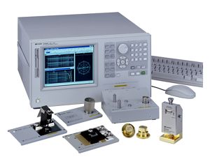
E4291A RFインピーダンス/マテリアル・アナライザは、表面実装コンポーネントや誘電/磁性材料を高確度に測定できます。4291Bは反射測定法ではなく、電流-電圧測定法を使用しているため、広範囲のインピーダンスを正確に測定することができます。
基本インピーダンス確度は、± 0.8%で、Q確度が高いため、低損失コンポーネントの解析が可能です。内蔵シンセサイザは、1 MHz~1.8 GHzの周波数を1 mHz分解能で掃引できます。またケーブルは、1.8 mの誤差の少ないケーブルを使用しており、確度を犠牲にせずにテスト・ポイントとアナライザの距離を離すことができます。さらに高度な校正および誤差補正機能により、測定治具内の測定誤差要因を取り除いて、DUT/MUTで優れた確度と再現性を実現できます。
4291BではIBASICを用いて、レベル制御とテスト信号のモニタを自動的に行え、一定の電圧/電流でデバイスを測定することができます。オプションのDCバイアス(最大40 Vおよび100 mA)を使用すれば、バイアス依存のインピーダンス測定が行えます。また内蔵の等価回路解析機能により、ワンボタンで、5種類の回路モデルの回路定数が自動的に計算されます。
4291Bは2個の測定チャネルを備え、各チャネルを1つ(たとえば、Z)または2つ(たとえば、Z‐θ)のインピーダンス・パラメータ測定用に設定することができます。またカラーTFTは分割表示でき、アクティブ・トレースとメモリ・トレース(RAMに保存された)の両方を表示できます。内蔵のフロッピー・ディスク・ドライブは、プログラムやテスト・データをLIF/MS-DOSフォーマットで保存できます。 内蔵のIBASICにより、恒温槽やウェーハ・プローバなどの外部テスト機器を4291Bから直接制御することもでき、専用の測定器コントローラは必要ありません。
材料評価
4291Bを使用すると材料の評価が容易に行え、材料評価の品質および効率が向上します。4291Bは包括的な誘電/磁性材料測定ソリューションを広い周波数範囲(1 MHz~1 GHz)で実現しています。
◆4291Bの詳細仕様(データシート)は、 こちらから(5.45MB)
◆関連マニュアルは、 こちらから
◆関連FAQは、 こちらから