


- Overview
- All Models
- Support
High-isolation switching for ultra-low current, high-impedance testing
Keysight low-leakage switch matrices are designed for automated semiconductor testing that demands ultra-low current measurement and high isolation performance. Engineered to maintain signal integrity at femtoamp levels, these switch matrices enable seamless switching across multiple devices or test nodes without compromising measurement accuracy. With flexible configurations, compact form factors, and easy integration with Keysight analyzers, they are ideal for parametric testing, reliability studies, and wafer-level characterization. Request a quote for one of our popular configurations today. Need help selecting? Check out the resources below.
Femtoamp-level isolation
Maintain the integrity of ultra-low current measurements with switch paths designed to minimize leakage, ideal for precision measurements in advanced semiconductor materials.
Flexible channel expansion
Accommodate complex test configurations with scalable channel counts up to 48 outputs, supporting multi-pin devices and automated test matrices in wafer-level setups.
Capacitance correction design
Ensure accuracy in high-impedance CV testing with dedicated capacitance compensation paths that reduce distortion in sensitive device measurements.
Seamless integration
Easily combine with parameter analyzers and semiconductor device test systems, controlled via intuitive software interfaces for automated switching routines.

-
Minimum current measurement resolution
1 fA to 20 fA
-
Maximum output ports
48 to 96
-
Isolation
10 TΩ to 100 TΩ
-
Type
Matrix, Matrix or Multiplexer
Most popular configurations
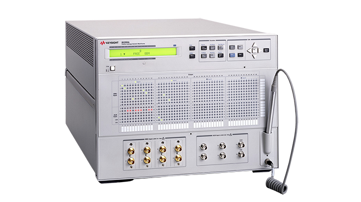
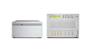
Low Leakage Switch Mainframe
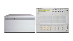
fA Leakage Switch Mainframe
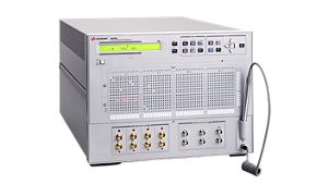
Low-leakage Switch Mainframe
- The Parametric Measurement Handbook
- Impedance Measurement Handbook
Services and support
Innovate at speed with curated support plans and prioritized response and turn-around times.
Get predictable, lease-based subscriptions and full lifecycle management solutions—so you reach your business goals faster.
Experience elevated service as a KeysightCare subscriber to get committed technical response and more.
Ensure your test system performs to specification and meets local and global standards.
Make measurements quickly with in-house, instructor-led training, and eLearning.
Download Keysight software or update your software to the newest version.
Frequently asked questions
A low-leakage switch matrix is a specialized signal routing system designed to connect precision instruments such as source measure units (SMUs), LCR meters, or capacitance measurement units to multiple device terminals in a highly controlled and electrically isolated manner. These systems are optimized for high-impedance measurements and ultra-low current switching, typically in the femtoamp (fA) range. The matrix allows seamless automation of multi-pin device testing, wafer probing, and reliability analysis without compromising the signal integrity required for sensitive IV or CV measurements. By enabling unattended switching between device pins, a low-leakage switch matrix minimizes the need for manual reconnections, thereby reducing measurement errors, contamination risk, and test time.
Leakage current can introduce significant errors when measuring ultra-small signals, particularly in advanced or scaled semiconductor devices such as gate oxides, passivation layers, thin dielectrics, and novel materials like organic semiconductors or 2D materials. In such contexts, target currents may be on the order of femtoamps or picoamps, and even minuscule leakage through switch relays, cabling, or connectors can distort results. High insulation resistance (typically >100 TΩ), low dielectric absorption, and optimized guarding are essential for maintaining signal purity. Low-leakage switch matrices are constructed with Teflon or ceramic substrates, guarded triaxial paths, and specialized relay designs to suppress parasitic current paths and maintain the integrity of these delicate measurements.
Low-leakage switch matrices are typically integrated with parametric test systems, semiconductor device analyzers, and wafer probers for automated electrical characterization. Each matrix channel connects device terminals to instruments in a programmable fashion via software, enabling rapid reconfiguration during test sequences. This integration supports advanced test routines such as Kelvin sensing, differential measurements, and multi-terminal IV/CV sweeps. The matrix is often controlled via SCPI commands, GUI-based software (such as EasyEXPERT), or automation frameworks in high-throughput environments. Features like crosspoint switching, relay matrix mapping, and high-speed actuation allow seamless coordination between switching and measurement instruments, minimizing idle time and maximizing throughput during wafer-level testing or reliability analysis.
Several critical parameters influence the selection of an appropriate switch matrix for semiconductor applications:
- Channel count and configuration: Determine the number of inputs (instrument ports) and outputs (device connections) needed for your application. Some models support up to 48 outputs with configurable routing (e.g., 4x12, 8x6).
- Leakage current and isolation resistance: For ultra-low current testing, select a matrix with sub-femtoamp leakage and insulation resistance exceeding 100 TΩ to avoid measurement distortion.
- Bandwidth and capacitance: High-speed CV measurements or RF probing require adequate signal bandwidth and low parasitic capacitance. Some matrices support bandwidths up to 30 MHz.
- Contact resistance and relay lifetime: Choose systems with low, stable contact resistance and long-life reed or solid-state relays, especially for production or stress testing environments.
- Capacitance compensation and guarding: Look for dedicated features such as active guarding paths or capacitance correction lines to preserve signal fidelity in high-impedance setups.
Relay and shielding design are central to a switch matrix’s ability to maintain high-fidelity signal paths. Electromechanical relays in low-leakage matrices are selected for their high insulation resistance, low stray capacitance, and low dielectric absorption. Many systems use reed relays encased in hermetically sealed glass to minimize contamination and improve long-term stability. Additionally, shielding techniques such as driven guards, triaxial cables, and isolated signal paths protect sensitive measurements from external interference and ground loops. Internal PCB layouts often include ground planes and guard traces to control leakage paths and signal coupling. Proper shielding ensures that the matrix itself does not become a source of error, especially when measuring high-impedance nodes or performing CV characterization at low frequencies.