What are you looking for?
What Is the Finite-Difference Time-Domain Method?
Definition of the Finite-Difference Time-Domain (FDTD) Method
The Finite-Difference Time-Domain (FDTD) method is a rigorous and powerful tool for modeling nanoscale optical devices. FDTD solves Maxwell’s equations directly without any physical approximation, and only the extent of the computing power available limits the maximum problem size.
Table of Contents
How Does FDTD Work and What Problem Does It Solve?
The FDTD method solves Maxwell’s equations on a mesh and computes E and H at grid points spaced Δx, Δy, and Δz apart, with E and H interlaced in all three spatial dimensions. FDTD includes the effects of scattering, transmission, reflection, absorption, and so on. FDTD is a time-domain solution, but you can also perform frequency analysis through the use of the Fast Fourier Transform (FFT) and the Discrete Fourier Transform (DFT).
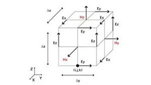

Figure 1. FDTD Yee cell of dimension Δx, Δy, Δz. [3]
When Would You Use FDTD Compared to Other Techniques?
FDTD can simulate any structure where Maxwell’s equations describe the necessary physics. Typical applications for this method include LEDs, solar cells, filters, optical switches, semiconductor-based photonic devices, sensors, nano- and micro-lithography, nonlinear devices, and meta-materials (negative index of refraction). Read about FullWAVE FDTD for details about additional applications.
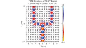

Figure 2. FDTD simulation of Y-branch PBG splitter.
What Software Models FDTD?
Keysight offers several photonic solutions tools that employ the FDTD method.
Keysight’s FullWAVE FDTD simulation software, part of RSoft Photonic Device Tools, employs FDTD to perform a full-vector simulation of photonic structures. Its award-winning, innovative design and feature set has made FullWAVE FDTD the market leader among optical device simulation tools, with a cutting-edge implementation of a mature FDTD algorithm that allows for a wide range of simulation and analysis capabilities. For a wide range of integrated and nano-optic devices, FullWAVE FDTD has applications such as LED extraction analysis, diffractive optical element (DOE) design, PIC/Custom PDK element design, nanophotonics, and meta-materials design.
FullWAVE FDTD example: modeling a surface-plasmon-based spatial multiplexer
The speed of intra-chip and inter-chip connection is one of the main bottlenecks to achieving faster computer chip performance. Routing the signals through surface-plasmon-based waveguides provides one possible way to achieve faster optical connection speeds; these waveguides are compact, not bound by the diffraction limit, and can easily integrate with both optical and electronic technologies.
One basic challenge facing the adoption of plasmon guides within electrical chips is the excitation of the plasmons from external sources. Simulating this effect requires a rigorous full-vector modeling environment that provides accurate solutions for arbitrary device geometries containing both metallic and nonmetallic components.
FullWAVE FDTD is the ideal tool to meet this need. FullWAVE provides a full-vector solution to Maxwell’s equations and allows engineers to use complex material definitions, arbitrary device geometries, nonuniform grids, and sophisticated measurement techniques to create new plasmonic devices and fine-tune existing designs for specific applications. You can also perturb the design parameters of the structure in FullWAVE FDTD to study manufacturing tolerances on device performance.
The surface-plasmon-based spatial multiplexer in Figure 3 consists of a multiplexing switch that steers light toward one of several subwavelength metal-strip waveguides. FullWAVE FDTD performed several 3D simulations at a fixed wavelength and at various incident angles of the illumination to determine the optimal angles at which light is coupled into each of the three metal-strip waveguides.


Figure 3. Schematic of the surface-plasmon spatial multiplexer.
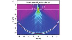

Figure 4. Simulation results showing the amplitude of the Ey field on the surface of the metal film: a) Normal incidence light (shown above) is coupled into the central metal-strip waveguide; b) Angled incident light is coupled into one of the side metal-strip waveguides.
The use of surface plasmon resonances in chip interconnects can allow for much faster chip performance. As shown in this example, rigorous simulation software like FullWAVE FDTD provides the necessary tools to study all factors that contribute to the design of a surface plasmon device.
For another example, read how FullWAVE FDTD simulates a q-plate.
Discover Keysight Photonic Solutions
Learn how to apply FullWAVE across applications, including light-emitting diode (LED) extraction analysis and more.

References
1] J.P. Berenger, “A perfectly matched layer for the absorption of electromagnetic waves,” J. Comput. Phys., 114, 185 (1994)
[2] A. Taflove, Computational Electrodynamics: The Finite-Difference Time-Domain Method (Artech House, Norwood, MA, 1995)
[3] K.S. Yee, “Numerical solution of initial boundary value problems involving Maxwell’s equations in isotropic media,” IEEE Trans. Antennas Propagat., AP-14, 302 (1966)
[4] A. Imre et al., "Multiplexing surface plasmon polaritons on nanowires," Applied Physics Letters 91 083115 (2007)
Access additional resources





Want help or have questions?