What are you looking for?
AI Compute
Test AI chips and high-speed digital designs.
Accelerate AI Semiconductor Testing and HSD Design
Unlock the future of AI-ready semiconductors and high-speed digital (HSD) designs. Design and test AI chips, troubleshoot cutting-edge designs, and meet or exceed the latest PCIe, DDR, and CXL standards with advanced design, debugging, and compliance tools — optimized for AI data centers.
Elevate Your Knowledge in AI Compute


5 Strategies to Optimize and Scale AI Data Centers
AI is transforming industries and driving innovation. That means network architects must manage increasing data center demands — including unique traffic patterns, dynamic workloads, and relentless performance pressures.
Read this eBook to discover five practical solutions to optimize AI data center performance for modern applications.


Accelerating AI Innovation with Concurrent Design Engineering
Designing AI chips is getting more difficult due to technical and economic hurdles like complexity, cost, and power consumption. Read this eBook to learn how to accelerate AI chip development across chiplet design, 6G research, power delivery, and engineering lifecycle management.


The Evolution of PCIe® Standards and Test Requirements
Data centers face increasing demands to achieve faster speeds — and AI is accelerating demand. As Ethernet speeds push past 800GE, PCIe® 6.0, the latest iteration of the Peripheral Component Interconnect Express® (PCIe®) standard, is accelerating data center innovation.


Digital Design and Interconnect Standards
When digital signals reach gigabit speeds, “the unpredictable” becomes normal. And when it comes to digital standards, every new generation and technology advancement puts new obstacles in your path. Explore tools for simulation, measurement, and compliance to cut through the challenges of gigabit digital designs.
Design and test AI chips and semiconductors
Accelerate design cycles, anticipate compliance challenges, optimize electronic performance, and deliver market-leading innovations faster.
Troubleshoot AI-optimized high-speed digital designs
Reduce design spins, test AI semiconductors, and analyze printed circuit board (PCB) performance with accurate, high-performance instruments.
Meet or exceed the latest AI networking standards
Simplify and accelerate compliance testing with automated test solutions for leading AI data center standards — including PCIe®, CXL, and DDR.
Test AI Chips and Debug HSD Designs with Keysight

Debug AI-ready designs with unmatched signal integrity
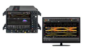
Reduce prototyping cycles, accelerate time to market, and improve data center infrastructure reliability with Keysight UXR B-Series oscilloscopes. Troubleshoot physical layer performance with the highest signal integrity measurements to build high-speed devices for the AI data centers of tomorrow.

Ensure compliance with next-gen AI compute standards
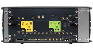
Characterize receivers and server interfaces for AI data center networks with Keysight Bit Error Ratio Testers (BERTs). Improve pathfinding for 1.6T and cutting-edge applications with uncompromising signal integrity, NRZ / PAM4 / PAM6 / PAM8 support, and data rates up to 120 Gbaud.

Accelerate design development at 160 Gbaud and beyond
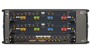
Keysight arbitrary waveform generators (AWGs) offer the speed, bandwidth, and precision to meet the demands of AI semiconductor testing and AI data center deployments. Test high-density communications, characterize design performance, and stress devices to their limits.


Get a clear and accurate view of PCIe® link traffic
Perform deep protocol analysis on PCIe® systems with unparalleled signal integrity. Keysight's PCIe Protocol Analyzer emulates and visualizes data traffic, pinpointing issues to validate hosts and endpoints for AI data center readiness — all in a pluggable, cable-free form factor for quick calibration.


Streamline design workflows with EDA products
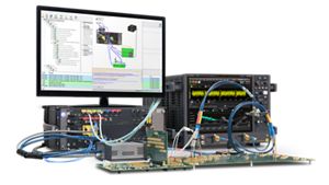
Simplify multi-domain insights throughout the design cycle with Keysight electronic design automation (EDA) products. Predict design challenges, simulate AI chips and semiconductor models, and deliver first-to-market products with design templates, component libraries, robust modeling, and precise simulations.
The Road to PCIe® 7
Are you ready to embrace the future of data transfer? PCIe® 7 and CXL offer faster data rates for high-performance applications, such as AI and machine learning. New technologies, such as PAM4 signaling at 32Gbaud, are a significant leap from older NRZ-based technologies — necessitating strict tolerances, evolving specifications, and new component models.
In this webinar, you will learn about the challenges of designing for these standards and explore simulation-driven compliance solutions using Method of Implementation (MOI) workflows to certify compliance tests.


Use Cases for AI Compute Testing and PCB Validation

Analyze PCB Signal Integrity
Reduce signal integrity risks in a high-speed digital PCB through the detection and diagnosis of crosstalk, jitter, vertical noise, and phase noise.

Perform PCle® 6.0 Protocol Validation
Achieve protocol validation at the physical, data link, and transaction layers.

Test DDR5 Transmitter Compliance
Execute a wide range of conformance tests based on JEDEC standards.

Test PCIe® 6.0 Receiver Compliance
Calibrate stress signals and test for PCIe® receiver compliance.
Learn More About AI Compute


Frequently Asked Questions: AI Compute
As data centers scale to support exponential traffic growth, the AI compute infrastructure they rely on — including CPUs, GPUs, accelerators, and memory interfaces — requires more rigorous testing. Validation must now address ultra-high-speed digital interfaces such as PCIe, CXL, DDR, and HBM, which are foundational to modern data center performance. Semiconductor testing is evolving with advanced tools like Keysight’s real-time compliance oscilloscopes, protocol analyzers, and BERTs to validate physical layer integrity and compliance under data center-level stress conditions. Testing now prioritizes signal integrity, performance, power efficiency, and reliability across dense server and custom silicon deployments.
Modern data centers are built on complex chipsets with tight timing margins and massive throughput requirements. Advanced semiconductor test tools — such as Keysight’s AWGs, high-performance oscilloscopes, and receiver test software — provide precision signal generation and analysis to ensure reliable high-speed capabilities. These tools help detect jitter, signal degradation, and signal quality across memory and I/O subsystems. For hyperscalers building custom chips for workloads like AI compute, storage, networking, and virtualization, these testing solutions accelerate qualification and reduce system-level issues post-deployment. Ultimately, enhanced validation means fewer failures in the field and improved uptime for data center services.
Data center chip development demands fast cycles and high-volume throughput. Reducing test time and cost depends on intelligent test coverage, efficient use of automated equipment, and robust simulation early in the design phase. Keysight’s EDA bundles — including tools like SIPro (signal integrity analysis) and System Design — allow engineers to simulate and validate high-speed channels before tape-out. On the bench, instruments like BERTs and real-time compliance oscilloscopes streamline compliance and debug for PCIe / CXL and memory interfaces, reducing costly rework and accelerating time-to-deployment.
Validation of data center compute systems requires a mix of physical layer measurements, protocol compliance data, and environmental stress data. Test engineers gather real-time performance metrics such as bit error rates, eye diagrams, TDECQ, jitter tolerance, and lane margining from equipment like BERTs, oscilloscopes, and AWGs. Additionally, simulation data from tools like Keysight’s PHY Designer or RF Circuit Simulation Professional is used to verify behavior under worst-case conditions. This data is critical in ensuring that server chips, memory modules, and interconnects operate reliably at scale and under the demanding workloads typical of hyperscale environments.
As data center AI compute designs push bandwidth limits and shrink power margins, engineers face challenges in signal integrity, protocol compliance, and thermal stability. Testing chiplets, stacked memory, and custom I/O paths — often across multiple voltage domains — requires precise tools and deep protocol visibility. Integrating high-speed validation into workflows without disrupting yield or time-to-market is also difficult. Tools like Keysight’s Design Data and IP Data Management help track test coverage, while protocol analyzers and advanced simulation suites reduce late-stage surprises. Ensuring the scalability of test setups across evolving interconnect standards like PCIe 6.0 and CXL 3.0 is an ongoing concern.
Key trends include the rise of composable and disaggregated architectures, adoption of chiplet-based designs, and custom silicon for power optimization. Best practices for testing data center AI compute include starting with simulation (using EDA tools like SIPro), leveraging compliance test automation on real-time oscilloscopes and BERTs, and correlating bench-level results with system-level performance. Hyperscalers are increasingly bringing testing in-house for greater control and faster iteration, using integrated validation platforms that combine physical, protocol, and data management layers to deliver faster, more reliable AI compute at scale.
Want help or have questions?