How to Maximize Inline IC Structural Screening Coverage

Maximize Inline IC Structural Screening Coverage
Maximizing inline IC structural screening coverage is essential for identifying semiconductor package defects, improving manufacturing quality, and reducing the risk of defective devices reaching customers. Keysight Inline structural screening evaluates semiconductor packages during manufacturing by measuring electrical characteristics that reveal structural abnormalities before final functional testing. This approach complements conventional Automated Test Equipment (ATE) and Automated X-ray Inspection (AXI) by helping identify structural defects that may not be detected through conventional open-short testing or limited sampling inspection.
Capacitive sensing techniques analyze the electrical coupling between internal conductive structures, such as lead frames and wire bonds, to identify potential structural abnormalities. Statistical profile analysis compares each device's measurement results against established production baselines, enabling automatic detection of abnormal structural characteristics. By applying this approach across high-volume manufacturing lines, engineers can expand inline screening coverage, improve defect detection, and enhance production quality and reliability.

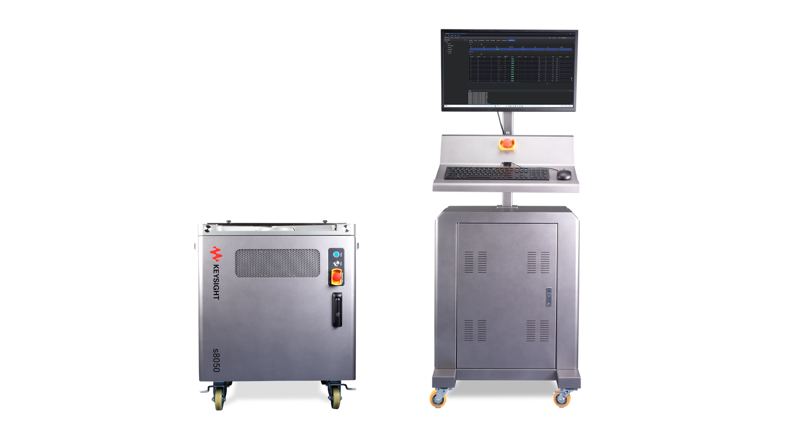
Inline Structural Screening Solution
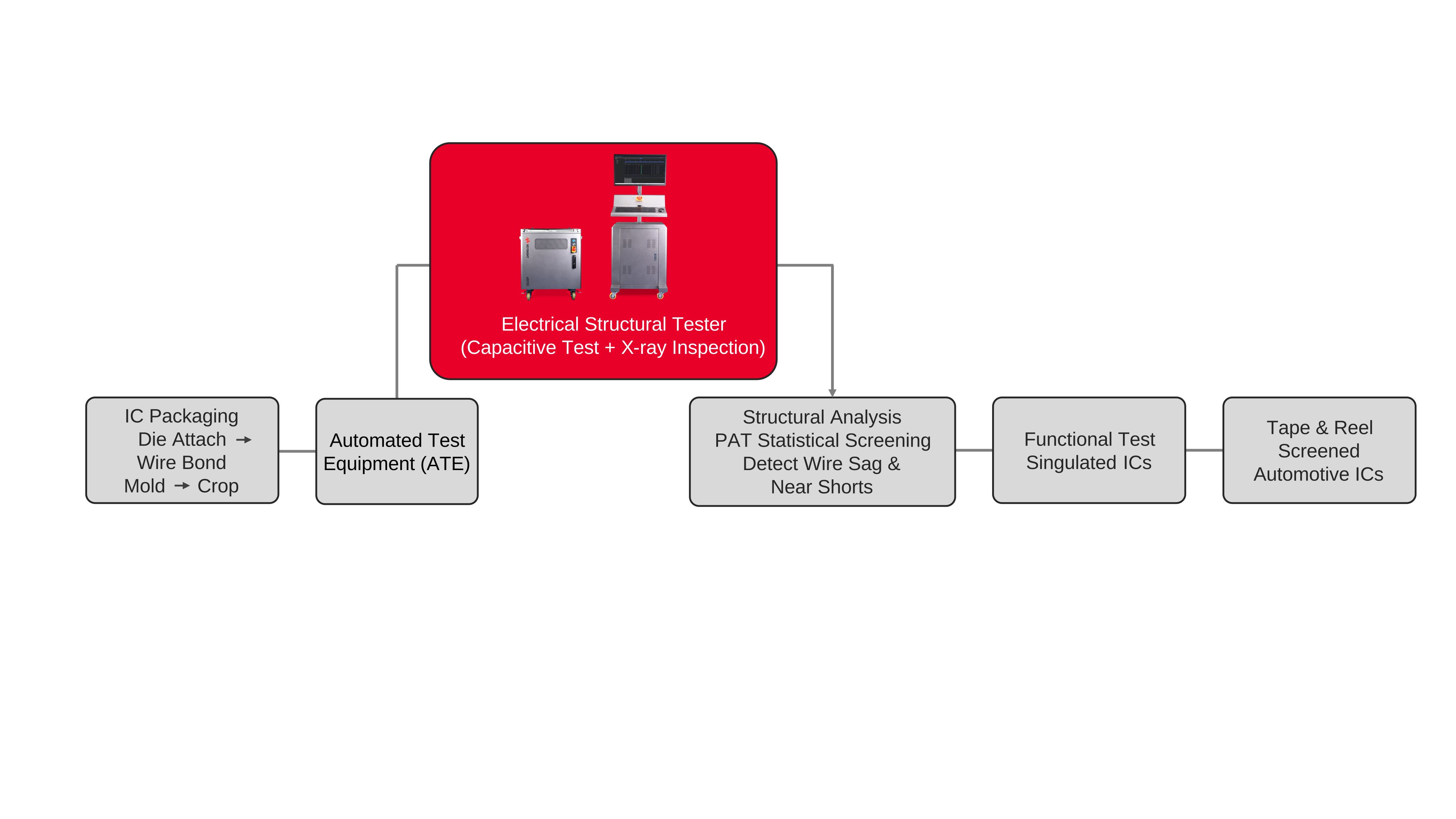
Achieving complete structural screening requires integrating a high-speed electrical inspection system directly into the semiconductor production flow without slowing manufacturing throughput. The solution combines Electrical Structural Testing with capacitive Vectorless Test Enhanced Probe technology to inspect internal package structures immediately after Automated Test Equipment testing.
The system detects structural defects including wire sag, near shorts, incorrect die placement, and abnormal package construction that may not be identified through conventional electrical or X-ray inspection alone. Built-in Part Average Test analysis continuously monitors production variations and dynamically updates screening limits to reduce false rejects. Supporting up to 20 parallel test sites and throughput reaching 72,000 units per hour, the solution enables full inline inspection for high-volume automotive semiconductor manufacturing while reducing escape defects and improving product quality.
See Block Diagram of Inline Structural Screening Solution

Explore Products in Our Inline Structural Screening Solution
-

![]()
Electrical Structural Tester


Discover Resources and Insights
Additional Resources for Inline Structural Screening
Related Use Cases


-
![]()
Learn More
How to Consolidate ICT and Functional Testing
Consolidate ICT, flash programming, and functional testing with the i7090 board test system to reduce test cycle time, simplify test operations, and improve production throughput.
Learn More

-
![]()
Learn More
How to Achieve Comprehensive Inline IC Structural Screening
Perform comprehensive inline structural screening of automotive integrated circuits using capacitive electrical structural testing.
Learn More
-
![]()
Learn More
How to Control ICT Tower Light Indicators
Control tower light and buzzer behavior in ICT systems to improve operator awareness, uptime, and manufacturing efficiency.
Learn More

Get in Touch with One of Our Experts
Need help finding the right solution for you?