


Why Use Photonic Device and Fiber Simulation
Advanced modeling and analysis for waveguides, optical fibers, and integrated photonic components.
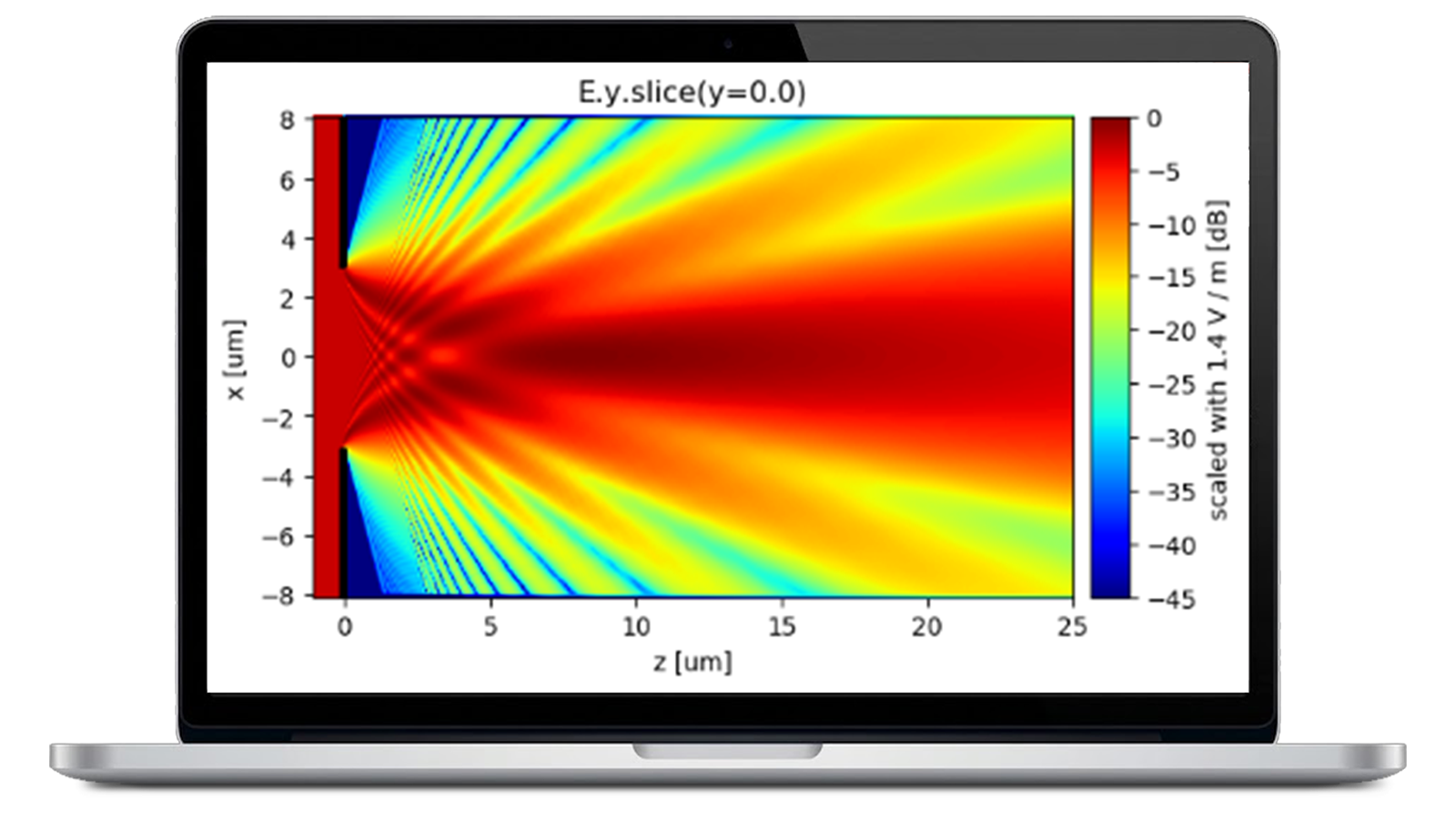
Developing innovative photonic devices requires accurate physics-based modeling, efficient simulation workflows, and powerful optimization capabilities. This solution provides a comprehensive design environment for the analysis and optimization of integrated photonic devices, waveguides, and optical fibers. Engineers can leverage advanced finite-difference mode solvers, beam propagation methods (BPM), and eigenmode expansion (EME) techniques to model complex 2D and 3D photonic structures with high accuracy. Flexible material definitions, customizable meshing, and realistic optical material models support detailed performance evaluation under real-world operating conditions. Integrated Python-based automation and advanced electromagnetic field analysis accelerate design exploration and optimization, while seamless integration with photonic circuit and fiber optic simulation environments streamlines end-to-end photonic development workflows. The result is faster innovation, improved device performance, and reduced design risk from concept through system integration.
Key Capabilities

Simulate photonic devices with advanced numerical solvers.

Analyze optical waveguide and fiber structures.

Model complex photonic device geometries accurately.

Visualize and manipulate calculated field distributions.

Automate workflows using integrated Python tools.

Connect device and circuit-level simulations seamlessly.
Resources to Get You Started
This brochure introduces VPIdeviceDesigner, a Python-based simulation framework combining finite-difference optical mode solvers, the Beam Propagation Method (BPM), and the Eigenmode Expansion (EME) method. It highlights capabilities for modeling complex geometries and optical materials, automating parameter sweeps, and analyzing electromagnetic fields. GDS layout exchange and export of device models support integration with photonic circuit simulation. Application examples include polarization converters, edge couplers, optical splitters, and plasmonic structures.


blogs
Completing Keysight's End-to-End Photonic Design Workflow
Brochures
Photonic Design Automation for Components, Systems & Networks

Have Questions? We've Got Answers
The software is used to analyze, model, and optimize integrated photonic devices, optical waveguides, and fiber structures for research and product development applications.
The platform includes full-vectorial, semi-vectorial, and scalar finite-difference mode solvers, as well as beam propagation method (BPM) and eigenmode expansion (EME) technologies.
Yes. Users can create and analyze realistic 3D device layouts, including complex geometries, advanced materials, and customized mesh configurations.
Yes. An integrated Python interface enables automation, optimization, custom analysis workflows, and integration with scientific computing libraries such as NumPy, SciPy, and Matplotlib.
The software integrates with photonic circuit, process design kit (PDK), optical system, and fiber optic simulation environments, enabling seamless multi-level photonic design and verification.