Choose a country or area to see content specific to your location
Können wir Ihnen behilflich sein?
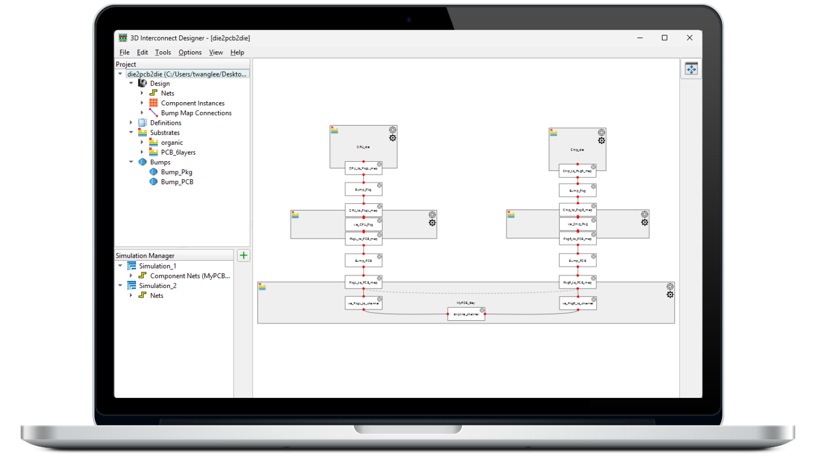
Design, model, and validate complex 3D interconnect architectures with a powerful standalone design environment.
Automate transmitter and receiver validation across next-generation I/O, memory, and fabric interfaces.
Strengthen 1.6T network reliability for AI-scale workloads from transceivers to interconnects.

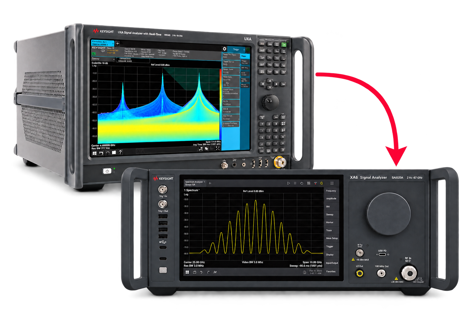
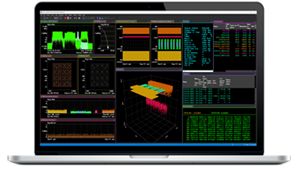
Pair Keysight VSA software with the new XA5 signal analyzer for advanced visualization, demodulation, and analysis — start your 30-day trial today.
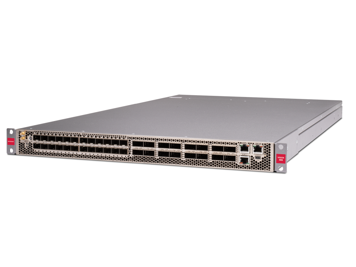
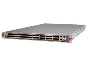
With extra memory and storage, these enhanced NPBs run Keysight's AI security and performance monitoring software and AI stack.
Explore end-to-end workflows spanning IC design, validation, wafer test, and photonics.

Save up to 50% on our latest instruments with eligible Keysight or competitor trade-ins.
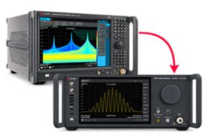
Maximize accuracy and performance with precision accessories engineered for Keysight instruments.
Save up to 50% on our latest instruments with eligible Keysight or competitor trade-ins.
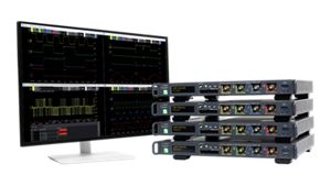
Four channels per 1U of rack space, up to 1 GHz bandwidth, and multi-oscilloscope synchronization.
Purpose-built solutions engineered for the design and test challenges unique to your industry.
Use Cases mapped to every stage of your product lifecycle, from design through operations.
Success Stories
Authoritative application notes, data sheets, reference designs, and test procedures to accelerate design and validation decisions.
Hands‑on bootcamps that teach system design, test methods, and production workflows engineers can apply immediately.
Learning Hub
Explore methodologies, test strategies, and technical resources for designing, validating, and scaling AI systems and networks.
Quick access to the most frequent support related self-help tasks.
Additional content to support your product needs.
Explore services to accelerate every step of your innovation journey.
Accelerate mission-critical system development with 3DHI based FEM and Phased Array designs, RF system simulation, SATCOM system modeling, and both ground-to-satellite and satellite-to-satellite optical link design.
Design and optimize 3DHI RF modules for radar, electronic warfare, phased arrays, and satellite systems with advanced multi-physics simulation and verification.
Streamline RF board development for phased arrays, avionics, and secure communications through automated co-simulation, design reuse, and manufacturing validation.
Design and verify phased array antennas for radar, electronic warfare, SATCOM, and sensing systems with beamforming, beam steering, and system-level simulation.
Optimize satellite links, RF subsystems, and phased arrays with high-fidelity modeling to ensure reliable aerospace communications and network performance.
Reduce deployment risk with RF digital twins that model realistic channels, RF impairments, and end-to-end network performance.
Simulate and optimize optical satellite links, evaluating performance, impairments, and design tradeoffs for reliable space communications.
Case Studies
Case Studies
Case Studies
Case Studies
Case Studies
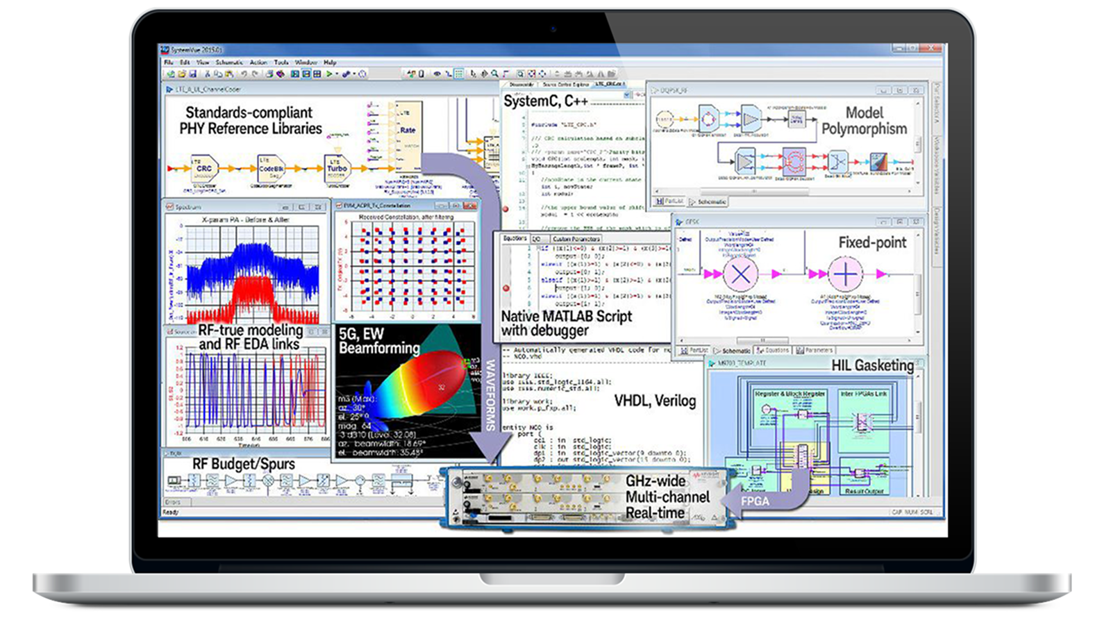
RF System Design (SystemVue) provides a scalable RF digital twin platform for the design, optimization, and validation of advanced wireless, satellite, radar, phased array, and Aerospace & Defense systems. Modern RF systems require accurate modeling of RF impairments, phased-array beamforming, propagation environments, nonlinear hardware behavior, and complex baseband processing across multiple domains. Traditional spreadsheet-based analysis and disconnected simulation tools cannot efficiently address the complexity of emerging wireless systems.
The operational requirements at Ka and Ku frequency bands rely on phased arrays' beamforming and steering capabilities. Engineers must optimize design and test cycle time to meet high-volume production demands in expanding markets. Phased array systems' extreme complexity and increasing system integration present many simulation and testing challenges. Keysight solutions cover the entire phased array workflow, empowering engineers to streamline design and testing processes.
blogs
blogs
blogs
blogs
blogs
This bootcamp demonstrates how to overcome the challenges of designing 3DHI RF Modules. Keysight ADS with RFPro provides the only fully integrated environment for RF 3DHI module and RF chiplet design, simulation, and optimization in complex systems.
This EDA bootcamp shows how to solve today’s design challenges resulting from RF applications operating at ever-higher frequencies and bandwidths.
See how electro-thermal heating alters device characteristics, degrades RF and Microwave circuit performance, and reduces reliability. Simulation replaces guesswork assumption of fixed ambient temperature settings for circuit simulation.
Dive deeper into the design (simulation) and test (validation) of phased array antennas.
This boot camp will explore the Keysight NTN ecosystem of solutions for modeling, simulation, and emulation.
Learn how to simulate and emulate an end-to-end satellite transmission chain using accurate channel, RF subsystem, and antenna models to reduce development time.
Webinars
eBooks
White Paper
White Paper
Solution Briefs
Solution Briefs
EDA software enables engineers to model, simulate, and optimize complex RF, microwave, satellite, photonic, and electronic systems before hardware is built, reducing development risk, cost, and schedule delays.
Digital twins create virtual representations of real-world systems, allowing teams to predict performance, validate requirements, evaluate mission scenarios, and connect simulation with measurement data for more accurate development decisions.
Yes. Engineers can simulate complete satellite communication chains, including RF subsystems, phased-array antennas, dynamic channels, beam management, and satellite handoff scenarios to improve connectivity and quality of service.
EDA tools support phased-array design through antenna modeling, beamforming analysis, digital beamforming impairment studies, coverage mapping, and system-level performance optimization before physical deployment.
EDA platforms model end-to-end non-terrestrial network links, transmission channels, antenna systems, and digital twin environments to evaluate performance across terrestrial, airborne, and satellite communications.
Integrated EDA workflows enable 3D heterogeneous integration, RF chiplet assembly, electromagnetic analysis, circuit co-simulation, and optimization within a unified design environment, helping identify issues early.
Engineers can accurately analyze RF paths, packaging effects, connectors, antennas, and enclosure interactions before fabrication, reducing costly design iterations and improving first-pass success rates.
Yes. Photonic design environments support modeling of amplifiers, modulation formats, signal-processing techniques, and optical transmission system impairments across complex communication architectures.
Engineers can simulate radar operations, satellite handoffs, communication coverage, beamforming performance, network behavior, mission planning, and hardware-in-the-loop validation within realistic operating environments.
A unified workflow connects RF circuit, electromagnetic, package, system, network, and photonic simulations into a single design process, improving collaboration, accelerating verification, and increasing confidence in mission-critical performance.
Talk to our team to find the right solution for your design needs, get a personalized quote, or request a free trial.
Können wir Ihnen behilflich sein?