
Designing Phased Arrays: Key Principles, Challenges, and Solutions
Find out why accurate phased array simulation and design are becoming increasingly critical in RF applications across Wireless, Cellular, and Aerospace/Defense industries.
Key takeaways:
- Electronically steered phased array antennas have become crucial for size, weight, and power reduction in multiple critical industries.
- Modern phased arrays can manipulate RF power into narrow beams that can be formed, steered, and shaped in any desired way.
- Keysight provides powerful solutions for virtual phased array simulation and design that shifts validation as far left as possible.
An antenna is an integral part of every device that uses radio frequencies (RF). Not that long ago, every mobile phone had a conspicuous antenna, and every satellite had a large movable dish antenna.
Fortunately, technical innovations have miniaturized antennas down to a few millimeters that can be fabricated on printed circuit boards. These phased array antennas are fully electronic without any mechanical elements, making them fast and durable.
In this post on phased array simulation and design, find out how phased arrays work, why they're becoming so critical to RF engineering, and how to efficiently design and test them.
What is a phased array antenna?
A phased array antenna (PAA) has multiple antenna elements that are carefully controlled to combine their RF power in desired directions. Power is boosted through constructive interference between signals and reduced in undesired directions through destructive interference.
Older PAAs used mechanical steering. Modern PAAs steer beams electronically without mechanical movements, making them less prone to failures. These are commonly called electronically scanned arrays (ESAs) and typically consist of a grid of small microstrip patch antenna elements.
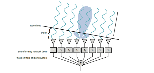
Figure 2. Phase shifting using delay lines
There are different approaches to phase shift individual elements. One simple method is to use delay lines that turn the elements on or off. During transmissions, they delay the source RF signal to each element. During receptions, they delay the received signals. Then all the signals are summed up. This process is called delay-and-sum.
What are the main types of electronically scanned phased arrays?

Figure 3. Passive and active ESAs
There are two main types of ESAs: passive ESA (PESA) and active ESA (AESA).
A PESA has a centralized architecture. All the elements and the baseband source are connected to a single pair of transmitter and receiver paths. While sending, a central powerful transmitter generates a high-power signal. It's fed into a power divider network and split into an identical copy for each element. Each signal passes through a separate electronically controlled phase shifter. A central beam steering controller tells each phase shifter exactly how much phase shift to apply.

Figure 4. Inside an active ESA
An AESA has a distributed architecture. Each antenna element has its own connected transmit power amplifier (PA), receive low-noise amplifier (LNA), phase shifter, attenuator, and switch. All are integrated onto a single transmit/receive (T/R) module connected to the patch antenna.
Role of a phased array antenna
Let's understand some of the key uses of phased array antennas that make them increasingly critical to RF designs across multiple domains:
- Beamforming: The radiation patterns from all elements combine to focus maximum power only in specified directions while minimizing power in all other directions, effectively forming beams of radiation. The directions of maximum power are called the main lobes or primary beams.
- Beam steering: The core function of a phased array is to electronically steer the main beam quickly without any mechanical movement. This enables rapid tracking and flexible searching.
- Beam shaping: The shape of the radiated power can be controlled by varying the signal amplitudes fed to each element.
- Multiple beam creation: A larger number of elements enables the simultaneous shaping and delivery of multiple beams. This has become essential for modern communication systems that track multiple targets or communicate simultaneously with multiple devices, ground stations, or satellites.
- Interference and jamming suppression: An adaptive beamformer can detect the direction of a jammer and place a deep null in that exact direction, effectively deafening itself to the jammer while still listening for the desired weaker signals from desired directions.
- Multipath fading mitigation: In dense urban environments, signals can bounce off buildings and other structures to create multiple copies of the same signal that interfere destructively and fade. An adaptive array can treat the unwanted reflections as interference and null them out or intelligently combine the paths to make the signal even stronger.
- Mission flexibility: Software-defined phased array antenna systems enable real-time function changes, like switching rapidly between radar and communication functions.
What are some key applications of phased arrays?
Some key current and anticipated applications of phased arrays are:
- Satellite communications: Satellite communications in the Ka (26.5-40 gigahertz or GHz) and Ku (12-18 GHz) bands heavily rely on beamforming and steering using phased array antennas. Non-terrestrial networks for telecommunications and internet satellite constellations like Starlink also rely on phased arrays.
- Telecommunications: Multipath fading mitigation using beamforming is essential for 5G/6G due to their use of higher millimeter-wave (mmWave) frequencies. Massivemulti-user multiple-input-multiple-output (MIMO) also heavily relies on beamforming.
- Defense: All modern radar systems use AESAs and PESAs for electronic warfare, jamming, and anti-jamming.
- Automotive: Automotive radar sensors use phased arrays for scanning their environments and estimating distances and sizes of obstacles. Accurate scanning enables better advanced driver assistance systems and vehicle-to-everything communications.
Modeling beamforming phased arrays

Figure 5. Radiation pattern for a 30° steered beam in Cartesian and equivalent polar charts with a main lobe and several side lobes (four are labeled for easy mapping between the two charts)
Since beamforming is one of the primary uses of phased arrays, let's understand relevant phased array simulation and design aspects below.
What are some key modeling principles for beamforming?
Beamforming modeling seeks to accurately determine these metrics:
- Optimal amplitude and phase weights: Optimizing complex beams requires calculating optimal amplitude and phase weights for each channel. This requires iterative numerical optimization to achieve a target beam width and effective isotropic radiated power (EIRP).
- System metrics: Key output parameters include EIRP, carrier-to-noise and distortion ratio, error vector magnitude, adjacent channel power ratio, gain over temperature, and third-order intercept point.
- System trade-offs: Modeling is used to evaluate design trade-offs, such as cost versus performance.
What are some challenges of modeling beamforming?
Some challenges that design and simulation tools must address are:
- Nonlinearities: Nonlinearities in amplifiers and mixers generate spurious radiation in undesired directions, potentially violating spectral emissions masks. Accurate modeling requires simulating nonlinear effects across hundreds of channels simultaneously.
- Quantization effects: In digital beamforming, the limited bit precision of phase shifters and attenuators introduces errors that significantly raise side lobe levels and affect beam width and directivity.
- Blind angles: Mutual coupling causes active impedances of array elements to change dynamically with the scan angle. If this impedance is mismatched with the preceding electronics, it leads to loss of directivity in specific directions called blind angles or scan blindness.
- Manufacturing variations: Variations in components (like gain, phase, and material properties) across the array must be modeled statistically to ensure reliable performance and graceful degradation from element failures. Techniques like Monte Carlo analysis are used.
- Multiple beam verification: Phased arrays can steer to thousands of beam positions, each requiring a separate pattern characterization. Faster techniques, such as near-field scanning and quick calibration methods, are essential.
- Over-the-air testing: Characterizing performance metrics using wideband modulated signals at mmWave frequencies is challenging due to high path loss. Sophisticated instruments and vector-corrected measurement techniques are needed.
- Computational load: As the number of array elements and the complexity of module integration increase, the electromagnetic simulation time also increases drastically. High-performance computing resources have become essential.
Designing a front-end module
Front-end modules (FEMs) are highly integrated RF subsystems with RF integrated circuits (RFICs), monolithic microwave ICs (MMICs), and others. In the context of phased arrays, they refer to the T/R modules connected to individual radiating elements.
Some key principles and challenges in FEM design are outlined below:
- Active impedance and load pull: Impedance of the array elements during beamforming and the resulting load pull on their power amplifiers can adversely affect the beams. These time-varying effects are quite unpredictable without high-fidelity modeling. For accurate modeling, a simulation tool like ADS is used to determine each PA's X-parameters. The full array's electromagnetic coupling matrix is determined using RFPro. Finally, the two results are combined using a system-level simulator like SystemVue.
- Nonlinearity: Amplifier nonlinearity generates spurious distortions that radiate in unwanted directions, increasing sidelobe levels and potentially violating radiation standards. Metrics like error vector magnitude and adjacent channel power ratio become crucial for validating the linearity and quality of modulated signals.
- Quantization errors: The use of discrete-value states by digital phase shifters and attenuators introduces quantization errors that affect the accuracy of beam steering and the sidelobe levels.
- Manufacturing variations: FEMs must be calibrated to compensate for relative gain and phase variances between channels that arise due to component manufacturing differences.
3D heterogeneous integration (3DHI) technologies in front-end modules

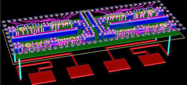
Figure 6. 3DHI for an FEM
Many RF front-end modules must comply with size restrictions, especially in compact devices like smartphones and automotive radars. This involves densely packing a large number of elements on a small FEM board, including phased array antennas, RFICs, MMICs, impedance matching networks, and systems-on-chip (SoCs).
One approach is to stack them vertically using 3DHItechniques. However, 3DHI complicates antenna patterns, electromagnetic interference, and thermal effects. Let's look at how 3DHI effects can be modeled, simulated, and mitigated.
The SmartMount feature in ADS enables physical designers to easily drag-and-drop components designed in different technologies into a single master layout. For example, Gallium Arsenide MMICs measured in microns, package substrates measured in millimeters, and laminate printed control boards measured in mils can all be added to the same layout. The tool automatically manages their scaling and technology mapping.
Designers can specify how ICs must be mounted relative to the package. SmartMount automatically handles the corresponding stackup and orientation.
After assembly, designers can use RFPro for electromagnetic simulations on the passive structures and combine their S-parameter results with active circuit models.
The integrated 3DHI model can then be imported into a system-level simulation tool like SystemVue to predict overall phased array performance while incorporating impairments like electromagnetic coupling, active impedance, load pull, and parasitics.
Modeling active impedance of the phased array load pull
This section explains the modeling of active impedance and load pull in phased array antenna designs.
What are active impedance and load pull?
Modern AESA designs impose highly dynamic loads on the integrated power amplifiers in their T/R modules.
Active impedance (also called Canning impedance) is the load impedance seen by an individual antenna element when the array is forming or steering a beam. It's caused by the applied amplitude/phase shifts and by the electromagnetic mutual coupling between array elements.
This dynamic impedance of an antenna element acts as the load on its connected PA and pulls it away from its optimal operating point. The load pull affects critical metrics like:
- gain and efficiency
- distortion and linearity
- S-parameters
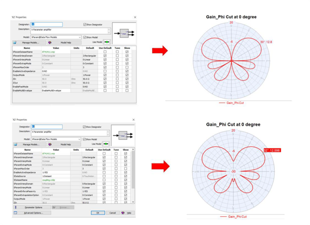
Figure 7. Beam deformation when active impedance modeling is enabled (bottom panel)
Active impedances and subsequent PA load pulls introduce complex time-varying effects during beamforming and steering. They can significantly affect the directions and shapes of the beams.
How can active impedance and load pull be accurately modeled?
First, a PA's non-linear behavior under varying loads is characterized by using circuit simulation tools like Keysight ADS. It employs harmonic balance simulations with swept input power and various load impedances. The output of this load pull analysis is used to generate the PA’s X-parameter matrix. X-parameters are crucial for high-fidelity modeling of dynamic load response as they describe non-linear behaviors, including impedance mismatches and harmonics.
Second, the entire array's S-parameter coupling matrix is derived from electromagnetic simulations using tools like Keysight RFPro.
Finally, the PA X-parameter model with load pull data and the array's S-parameter coupling matrix are imported into a system-level time-domain behavioral simulator like Keysight SystemVue. It iteratively simulates determining the antenna's port reflection coefficients and calculates the actual impedance seen by each PA, incorporating load pull and element coupling effects.
Additionally, for large phased arrays (100+ elements), the above array analysis workflow is computationally prohibitive. So a smaller representative subarray with unique coupling relationships is analyzed and then remapped to the full array.
In this way, by integrating PA load pull effects and active impedance calculations into a single time-domain behavioral simulation, designers can predict performance deviations accurately.
Keysight phased array simulation and design software
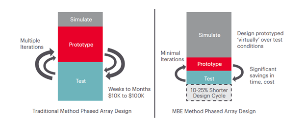
Figure 8. Keysight model-based engineering tools shorten design cycles and lower development costs
Keysight enables design teams to shift left most verification andoptimization as early in the design cycle as possible. Accurate system-level modeling software, powerful electronic design automation tools, realistic co-simulations of complex RF phenomena, and sophisticated test equipment for high-volume manufacturing are available from Keysight for RF engineers working on phased array systems.
Together, they enable extensive phased array simulation and design while minimizing the need for expensive, time-consuming hardware prototyping.
Features of the Keysight phased array design and simulation tools are explained in detail below.
System-level phased array design and simulation software
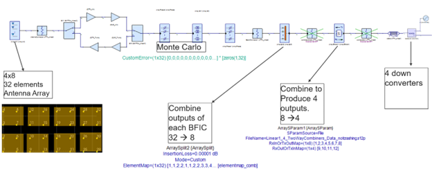
Figure 9. System-level modeling of phased array antenna and beamforming
SystemVue enables system-level design and simulation of patch antennas and front-end modules. Its digital-twin model-based engineering approach enables RF engineers to build detailed virtual prototypes that can explore the entire design space to construct an ideal topology that satisfies all specifications. It can model phased array antennas as well as higher-level designs like integrated circuits (RFICs), RF modules, RF boards, and transceiver systems.
Key capabilities are outlined below:
- Application-specific phased array configurations: Through the W4804B System Design Core, RF, Comms/DSP,Phased Array bundle, SystemVue can model phased array parameters specific to each application, like aerospace/defense, 5G/6G, and WiFi. The W4815B System Design Satellite bundle enables modeling of phased arrays for satellite communication systems.
- Ultra-fast simulations: The W4503EPhased Array Simulation engine enables powerful beamforming, time-domain, and frequency-domain analyses. Legacy RF simulators can take hundreds of hours just for computations. In contrast, system simulations with this engine run very fast, completing in just a few hours. Overall time savings are of the order of 200x and more.
- Fine-grained design space exploration: Designers can explore and verify the entire system design space. They can vary array topology parameters like the number of elements, array element patterns, inter-element spacing, frequencies, and more. For each parameter combination, they can simulate antenna gain, beam steering angles, amplitude/phase distributions, side lobe control, adaptive nulling, antenna element failures, and other specifications.
- Accurate impedance modeling: SystemVue models active impedance (Canning impedance) that's unique to phased arrays.
- Standards compliance: SystemVue eases the burden of complying with spectral emission mandates from standards and regulators. Spectral emission masks help find any violations in a simulation. They can be rapidly corrected at the system level, such as by modifying a filter after an amplifier, and the new design can again be quickly simulated.
EDA solutions for phased array design and simulation

Figure 10. 5G phased-array integration using Keysight ADS
The Advanced Design System supports detailed circuit, component, and multi-technology physical design, including 3DHI for phased-array and beamformer RFICs. It supports:
- multi-technology 3DHI, including chips, packaging, interconnects, shielding, boards, and I/O connectors
- circuit simulations
- electromagnetic simulations and co-simulations
- thermal simulations
RF Circuit Simulation Professional enables circuit and 3DHI simulation of phased array designs. RFPro enables 3D electromagnetic simulations of phased arrays using accurate finite element solvers. Both integrate seamlessly with ADS.
Rely on Keysight for effective phased array simulation and design
This blog post explained the uses of phased arrays across industries and introduced you to powerful phased array simulation and design tools.
Learn More
Phased Array Design and Test Learning Hub
3DHI and Phased Array webinar
RF System Design with Digital Twins Bootcamp
Design and Test a Phased Array Antenna Bootcamp
Phased Array Design White Paper
Related Posts