











- Overview
- All Models
- Support
Gain Visibility Into Device Behavior Through Optical Analysis
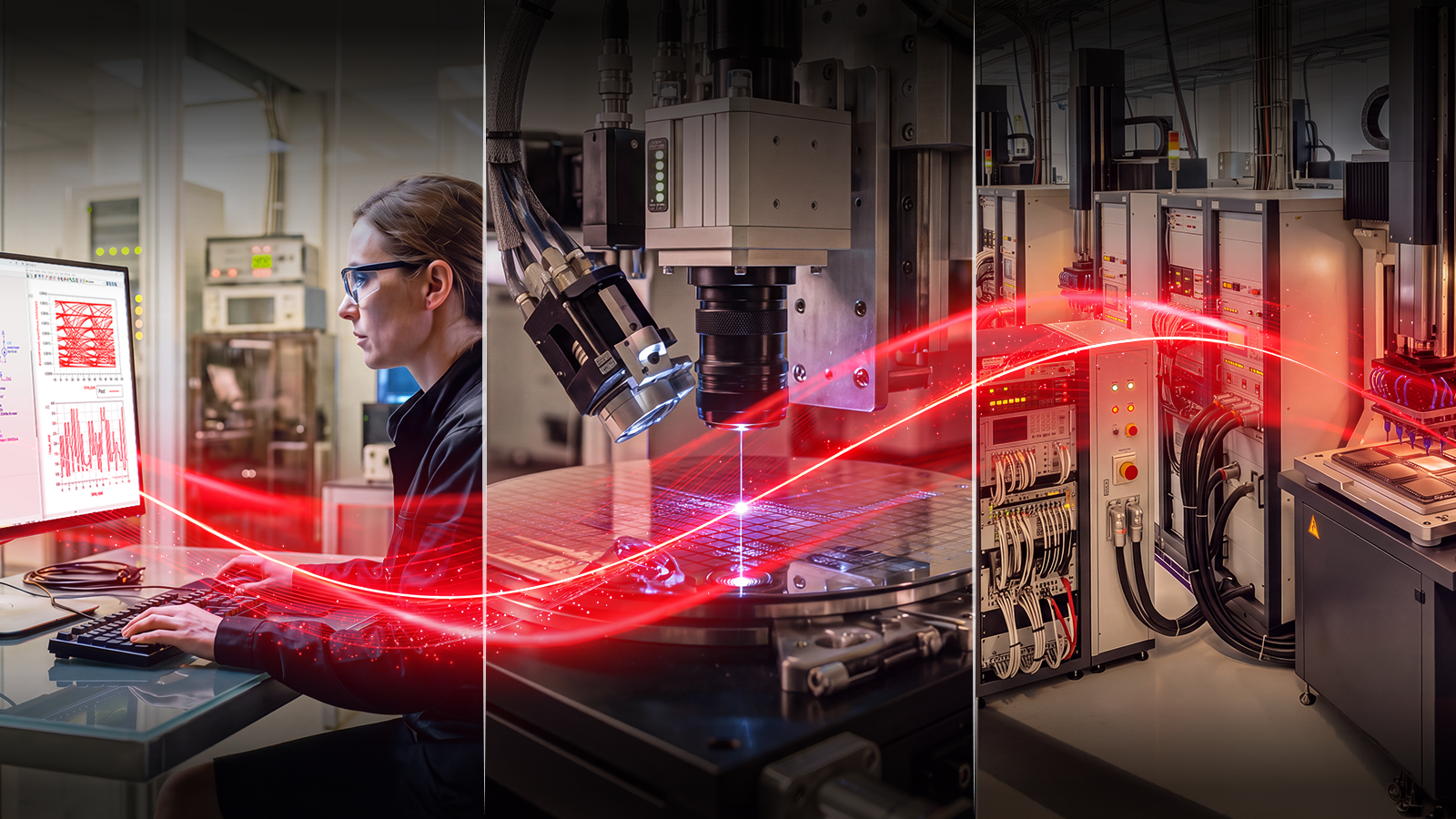
Optical analysis techniques provide a unique way to investigate the internal behavior of semiconductor devices through optical observation and measurement. By combining specialized laser sources, emission microscopy capabilities, and precision optical instrumentation, security engineers can identify areas of activity within a device and capture information that may reveal side-channel leakage or security-relevant behavior.
Unlike traditional side-channel measurements that observe power consumption or electromagnetic emissions, failure analysis methodologies leverage optical techniques to gain visibility into localized regions of a chip. This enables engineers to pinpoint active circuits, identify potential leakage sources, and better understand how security-critical operations are executed within silicon.
These techniques are commonly used to support vulnerability research, countermeasure validation, certification preparation, and advanced security evaluations. From locating areas of interest through photon emission imaging to performing optical side-channel measurements with precisely controlled laser sources, failure analysis tools help provide a deeper understanding of device behavior and support more targeted security investigations.
A complete failure analysis setup combines optical measurement, imaging, and localization capabilities within a single workflow. The DS1101A Fault Injection Laser System forms the core of the solution, providing the platform for precise optical investigation. Users can add either the DS1210A 1310 nm Single Mode Side Channel Laser Source or the DS1211A 1425 nm Single Mode Side Channel Laser Source to perform optical side-channel measurements, while the DS1105A Emission Microscopy Laser Station Adapter and DS1131A Emission Microscopy Extension Set enable photon emission imaging to visualize active regions of the chip. Together, these components help security engineers identify leakage sources, locate areas of interest, and gain deeper insight into device behavior.
Visualize Device Activity
Leverage optical techniques to observe and analyze active areas within semiconductor devices.
Identify Leakage Sources
Support Advanced Security Evaluations
Enable Precise Optical Measurements
Perform highly targeted investigations with laser-based analysis tools and emission microscopy capabilities.


-
Technology
Device Security
-
Wavelength
1425 nm, 1310 nm
-
Maximum output power
130 mW to 500 mW
-
Additional features
C-mount adapter for camera, 320 (H) x 256 (V) pixels with 30 in pixel size, squared, Active sensor size 9.6 mm x 7.7 mm, Frame rate 344 frames/s
-
Product type
Camera mount adapter, Side channel laser source, SWIR camera extension set
Most Popular Configurations
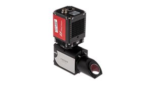

AV GoldEye G-008 InGaAS Camera
1310 nm Single Mode Side Channel Laser Source


1425 nm Single Mode Side Channel Laser Source
Services and support
Innovate at speed with curated support plans and prioritized response and turn-around times.
Get predictable, lease-based subscriptions and full lifecycle management solutions—so you reach your business goals faster.
Experience elevated service as a KeysightCare subscriber to get committed technical response and more.
Ensure your test system performs to specification and meets local and global standards.
Make measurements quickly with in-house, instructor-led training, and eLearning.
Download Keysight software or update your software to the newest version.
Frequently Asked Questions
Optical analysis uses specialized laser sources, imaging systems, and microscopy techniques to observe and investigate the internal behavior of semiconductor devices. These methods help security engineers identify areas of activity, locate leakage sources, and gain deeper insight into security-critical operations.
Power analysis measures variations in power consumption, while electromagnetic analysis measures EM emissions generated by device activity. Optical analysis provides visibility into localized regions of a chip, allowing engineers to observe activity within specific circuit areas and investigate leakage at a finer level.
Optical analysis is commonly used for:
- Vulnerability research
- Side-channel analysis
- Countermeasure validation
- Certification preparation
- Semiconductor security investigations
- Hardware security research
Optical techniques can provide visibility into specific regions of a chip that may be difficult to investigate using only power or electromagnetic measurements. They are often used as a complementary methodology to help localize leakage sources and better understand device behavior.
Optical analysis techniques can be used to investigate:
- Secure elements
- Smart cards
- Microcontrollers
- System-on-Chip (SoC) devices
- Cryptographic processors
- Other security-critical semiconductor devices
Yes. Optical analysis can help locate areas within a device that exhibit security-relevant activity and may contribute to side-channel leakage. This information can be used to guide further investigations using optical, electromagnetic, or power analysis techniques.
No. Optical analysis is typically used alongside power and electromagnetic analysis. Together, these techniques provide complementary insights that help security teams build a more complete understanding of device behavior and potential vulnerabilities.