












- Overview
- All Models
- Support
Non-intrusive test coverage for complex digital boards
Keysight boundary scan analyzers deliver advanced digital test capabilities for high-density boards, enabling precise fault isolation without requiring physical probe access. The system is designed for efficient structural testing and provides fast diagnostics of interconnects, shorts, opens, and stuck-at faults across complex digital assemblies. With seamless integration into in-circuit and functional test systems, boundary scan supports JTAG-based scan chains. It enables access to hard-to-reach nets, reducing test development time and improving coverage. Request a quote for the Keysight boundary scan analyzer today. Want to learn more about this solution? Explore the resources below.
Access hard-to-reach nets
Enables test coverage of hidden or inaccessible pins without physical probing, ideal for dense, multi-layer PCBs and fine-pitch components.
Fast, accurate fault isolation
Quickly detects and pinpoints opens, shorts, and stuck-at faults at the digital pin level, reducing debug time and improving yield.
Seamless integration
Easily integrate into in-circuit and functional test systems to expand coverage without adding complexity or increasing test time.
Non-intrusive structural testing
Performs structural diagnostics through standard test access ports (TAPs), eliminating the need for intrusive probing or additional hardware instrumentation.
-
System width
120 mm
-
CET ports
1
-
Tap IO ports
4
-
Remote test configurability
Yes
Typical configuration
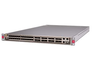
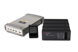
x1149 Boundary Scan Analyzer
- How Boundary Scan Improves Server Board Testing
- Enhancing Test Coverage Analysis with Boundary Scan
- How to Integrate Boundary Scan into In-Circuit Tester
Services and support
Innovate at speed with curated support plans and prioritized response and turn-around times.
Get predictable, lease-based subscriptions and full lifecycle management solutions—so you reach your business goals faster.
Experience elevated service as a KeysightCare subscriber to get committed technical response and more.
Ensure your test system performs to specification and meets local and global standards.
Make measurements quickly with in-house, instructor-led training, and eLearning.
Download Keysight software or update your software to the newest version.
Frequently asked questions
Boundary scan analysis involves testing the interconnects on printed circuit boards (PCBs) without using physical test probes. It leverages the IEEE 1149.1 (JTAG) standard to directly access and control pin states from the scan chain embedded in compliant devices. This technique is particularly valuable for modern PCBs with high-density components and limited physical access. Instead of probing pins, boundary scan manipulates the digital signals internally, detecting opens, shorts, and other structural faults. It is a powerful tool for early-stage prototype validation, board bring-up, and production testing.
Additionally, boundary scan analyzers support in-system programming of flash memories and FPGAs, which reduces the need for separate programming stations. Boundary scan is widely adopted because it allows efficient testing and debugging of complex board layouts, especially where traditional test methods are limited due to miniaturization and component packaging trends.
Traditional in-circuit testing requires physical contact with numerous test points on the PCB using bed-of-nails testers or flying probe systems. As boards become more compact and layered, reaching these test points becomes increasingly difficult and expensive. Boundary scanning eliminates much of this dependency by providing virtual access through scan-enabled components, drastically reducing the number of required test probes and fixture complexity. This leads to smaller, less expensive test fixtures and faster setup times.
With fewer mechanical interfaces to maintain and calibrate, ongoing maintenance costs also decrease. Because many tests can be reused or updated via software, modifications for new board revisions are more manageable and cost-efficient. This approach allows manufacturers to adapt quickly to design changes or test plan updates without incurring additional fixture redesign expenses, making boundary scan a highly scalable and cost-effective solution for both low- and high-volume production environments.
Yes. While boundary scanning is commonly used to detect open circuits and shorts between digital signal lines, its capabilities extend further when integrated into a broader test strategy. For instance, it can identify missing or incorrectly placed components by verifying the expected logical behavior of a circuit. It also aids in detecting stuck-at faults and specific signal integrity issues, particularly in digital communication buses.
When used with advanced tools or combined with functional test methods, boundary scan analysis can provide diagnostic feedback for specific devices like memory, logic gates, and programmable devices. It can also verify device orientation and connectivity across power and ground pins under some conditions. While it is not intended to replace all forms of electrical test (such as analog testing or complex functional verification), boundary scan analysis significantly enhances fault coverage in hard-to-access areas. It complements other strategies to improve overall board-level test reliability.
Boundary scan analyzers are well-suited for in-system programming (ISP) because they can directly access devices like microcontrollers, FPGAs, and flash memory via their JTAG ports or boundary scan interfaces. This enables device programming after being soldered onto the board, reducing logistical complexity and eliminating the need for pre-programmed components. The flexibility of in-system programming allows changes to firmware or configuration data late in the production cycle or even during field updates. It also facilitates automated manufacturing flows by embedding programming steps into test sequences, reducing operator handling time.
ISP through boundary scanning is particularly valuable in environments where multiple product variants are produced or when frequent firmware changes are required. It minimizes inventory risk and ensures that the latest firmware is always programmed during final test or board bring-up, improving efficiency and simplifying version control across the manufacturing process.
Yes. Boundary scan analyzers are highly effective for high-volume production, particularly where speed, repeatability, and automation are essential. Their software-driven nature allows easy integration with automated test equipment and manufacturing execution systems (MES). Once a test plan is developed, they can be reused across multiple units with minimal manual intervention. Boundary scan tests are typically fast, running in seconds, and do not require complex fixturing or manual probing, making them ideal for rapid throughput environments.
Boundary scanner diagnostic accuracy ensures that failures can be identified quickly, reducing time spent on rework and improving yield. Boundary scan analyzers also support real-time fault logging and analytics, which are increasingly crucial for Industry 4.0 initiatives. For large-scale manufacturers looking to optimize cost, quality, and efficiency, boundary scan analyzers are a proven solution that scales well from prototype validation to mass production.