Können wir Ihnen behilflich sein?
Device Modeling IC-CAP
Complete and accurate measurement control and parameter extraction solution for semiconductor device modeling
IC-CAP: The Industry Standard for Semiconductor Device Modeling
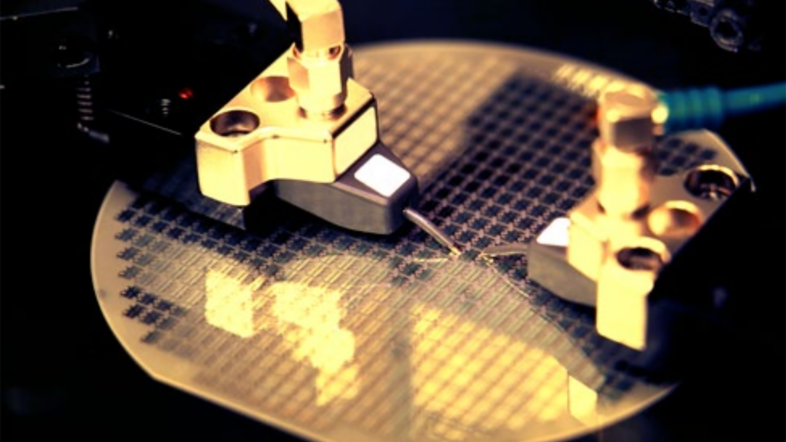
Device Modeling IC-CAP is the most advanced platform for semiconductor device modeling and characterization, trusted by foundries and fabless companies worldwide. It delivers accurate compact model extraction for high-speed/digital, analog, power electronics, and RF applications.
Why Choose IC-CAP?
- Streamlined Workflows
Simplify modeling for silicon CMOS, Bipolar, GaAs, GaN, and other advanced IC technologies. - Comprehensive Platform
Integrates measurement, simulation, optimization, and statistical analysis in one solution. - Open Architecture
Customize and automate measurement, extraction, and verification procedures for maximum flexibility.
Key Features
- AI-Powered Accuracy
Enhance automation and precision in device modeling workflows. - Turnkey Extraction Solutions
Pre-built flows for BSIM3, BSIM4, PSP, HiSIM, and other industry-standard CMOS models. - Seamless Integration
Direct links to major commercial simulators ensure consistency with circuit design environments. - Advanced Python 3 Experience
Built-in Python expanded package support for data processing, automation, instrument integration, and visualization.
IC-CAP Demo Videos
Find the Product That's Right for You

See also the W6325B PathWave MBP/IC-CAP Device Model Extraction and W6347B PathWave MQA/IC-CAP Modeling bundles.
Want more information on Device Modeling IC-CAP Products? View Configuration Guide
End-to-End Semiconductor Device Modeling Solution
Protect Your Innovation Investment


Innovate at speed by ensuring up-to-date application software & firmware and expert technical support at our fastest available times.


Software licensing, terms, and types
Keysight software licensing options provide flexibility and support. Choose your terms, choose your type, and keep control of your budget.


Manage your Keysight software, view and request licenses, and get the latest software updates.
Explore Semiconductor Device Modeling Use Cases


Helpful Resources on Semiconductor Device Modeling


Frequently Asked Questions
Semiconductor device modeling involves creating precise mathematical models that simulate the electrical behavior of semiconductor devices and circuits in response to various stimuli. A device model includes a set of equations with specific parameters or coefficients. Determining parameter values is a meticulous process that involves either direct extraction or optimization techniques to ensure the model equations closely fit the measured data.
Semiconductor device modeling forms the foundation of process design kits (PDKs), offering mathematical models that represent the behavior of the semiconductor devices, such as transistors, diodes, and capacitors, within the integrated circuits (ICs). As semiconductor device sizes shrink to the nanometer scale, device behavior becomes increasingly complicated as new physical phenomena occur. Accurate models enable design engineers to simulate and predict the behavior of devices before moving to costly physical prototyping.
Device modeling falls into the following categories:
- Physics-based models: Engineers recognize physics-based device models for their accuracy, as they rely on fundamental physical laws. One example is the 2D solution of Poisson's equation, which describes the electrical potential distribution in semiconductor devices.
- Empirical models: Derived by fitting equations to experimental data, these models prioritize practical predictability over theoretical foundations. For instance, the Curtice empirical model describes the I-V characteristics of metal-semiconductor field-effect transistors (MESFETs) and high-electron-mobility transistors (HEMTs).
- Semi-empirical models: These models combine physical principles with empirical data. For instance, Gummel-Poon is a semi-empirical model for bipolar junction transistors (BJTs).
- Table-based models: Table-based models, such as the HP Root FET model, interpolate measured data to simulate device behavior under different conditions.
- Artificial neural network (ANN) models: These models use artificial intelligence algorithms to learn from data and predict semiconductor device behavior. For instance, the DynaFET model applies neural networks to simulate the dynamic behavior and nonlinearities of field-effect transistors (FETs).
Modeling today’s industry-standard transistors is a complex and time-consuming process involving massive amounts of data. Extracting and verifying the quality of a Simulation Program with Integrated Circuit Emphasis (SPICE) model library can take weeks to months. As process technology advances, the model library needs continuous updates. Furthermore, the adoption of wide bandgap semiconductors relies on robust models for gallium nitride (GaN) devices to simulate highly nonlinear device behavior, including thermal and dynamic memory effects.
Semiconductor device modeling involves four basic steps to ensure accuracy and efficiency.
- Data measurement and analysis: This initial step measures the device’s physical and electrical properties, requiring extensive data collection. The procedure to select a typical die for measurements varies depending on the process development stage.
- Parameter extraction: This step involves extracting critical parameters such as DC, CV, S-parameters, and noise, which define the device's behavior under various conditions. The challenge for the modeling engineer is to implement a repeatable and robust procedure to extract the parameters of the model such that the mathematical model representation will match the measured data.
- Modeling: This step creates a mathematical model that accurately represents the device's behavior with the extracted parameters.
- Model validation: Validating the model ensures its reliability before it becomes available to users. Besides verifying the model's accuracy against measured data, modeling engineers must test its robustness by simulating it across multiple biases, geometry, and frequency conditions.
Want help or have questions?