What are you looking for?
What's New in High-Speed Digital Design and Simulation?
Watch the new demonstration videos below.
Keysight EDA’s High-Speed Digital Design Solutions for ADS 2027
ADS (Advanced Design System) 2027 continues to impress design engineers with cutting-edge technologies and capabilities that accelerate the path from design to product, delivering the highest design fidelity in high-speed digital applications. Featuring a robust, fully integrated design and simulation environment, ADS empowers engineers to efficiently create digital twins and manage the growing complexity of modern Chiplet Die to Die interconnects, Memory interfaces and SerDes systems—including USB, PCIe®, Ethernet and MIPI®. Its comprehensive solutions enable faster and more accurate simulations, advanced measurement techniques, compliance testing, and deeper insights, helping teams confidently address critical signal and power integrity challenges.
Highlights
ADS 2027 release for High-Speed Digital Designs introduces innovative and enhanced features and capabilities tailored for the following application areas:
- Chiplet Design
- Chiplet 3D Interconnect Designer
- Memory Design
- PCIe Design
- USB Design
- Ethernet Design
- MIPI Design
- SerDes Design
- Signal Integrity
- Power Integrity
- Electrical Performance Scan
- Design Cloud
Learn more:
Chiplet Design
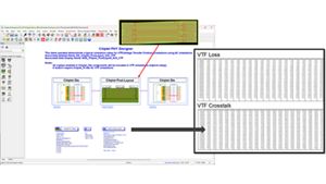
The Chiplet PHY Designer enables designers to predict the system-level end-to-end link margin with standard-specific measurements such as UCIe’s voltage transfer function (VTF) for the chiplet’s die-to-die interconnects. Built-in support ensures easy setup with key industry chiplet standards.
Highlights include:
- Latest standards: UCIe 3.0
- Supports QDR(Quarter-rate clocking)
- Supports UCIe and BoW (Bunch of Wire)
- Supports Pathfinding modes for UCIe and BoW


Chiplet 3D Interconnect Designer
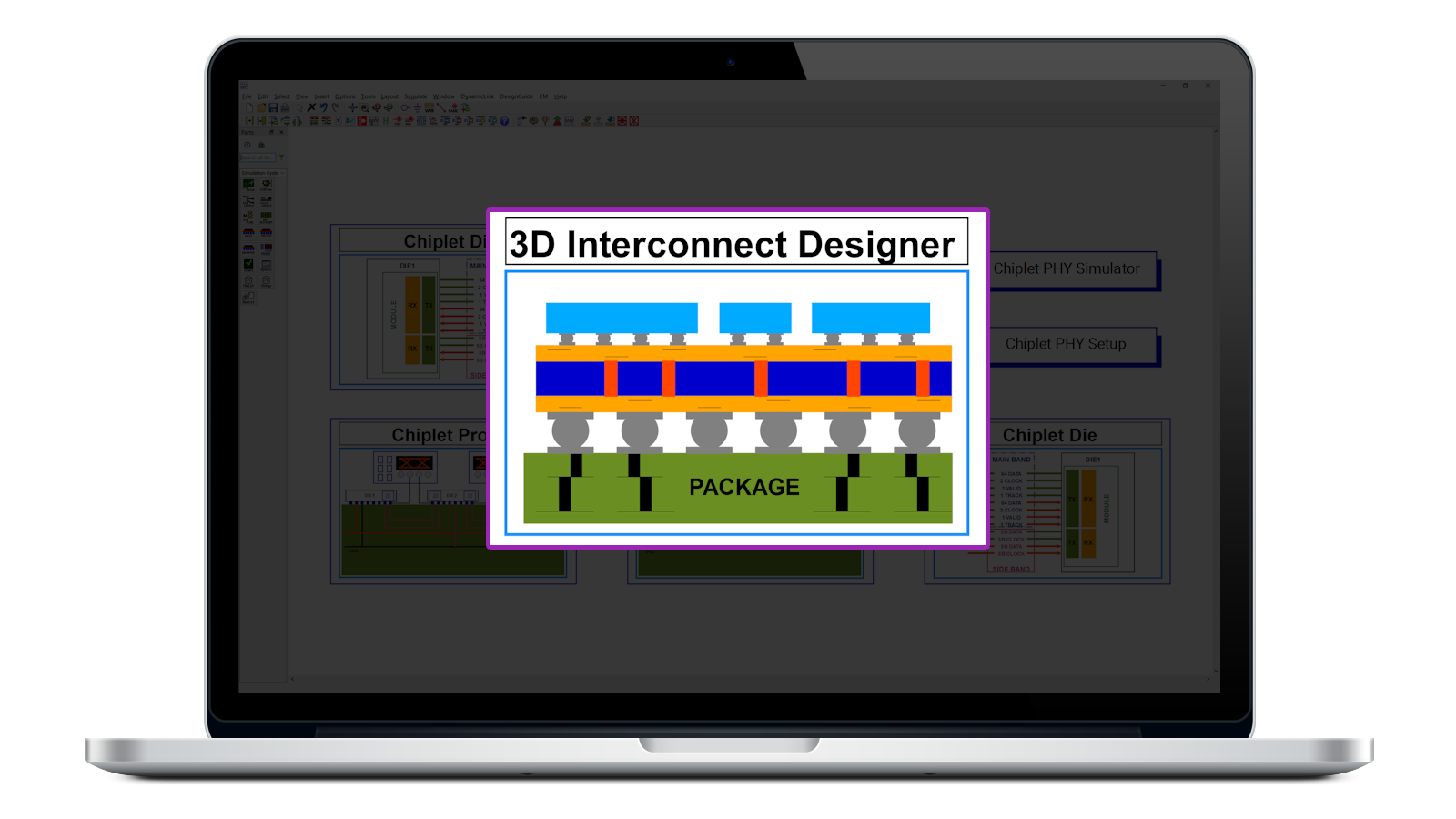
The Chiplet 3D Interconnect designer offers a pre-layout workflow solution that allows engineers to define, route and simulate their chiplet interconnect designs before committing to layout, enabling early validation and faster iterations.
Highlights include:
- Supports the design of organic and silicon substrates, including hatched ground planes.
- Supports UCIe and BoW standards and advanced package definitions.
- Supported interconnect types: microbumps, vias, and bus interconnects.
- Supports auto-routing of breakout regions and via structures.
- HTML report generation
- Python API support including python console
- Connect LLMs using the Model Context Protocol (MCP)
Memory Design
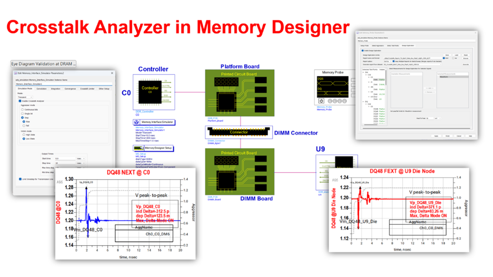
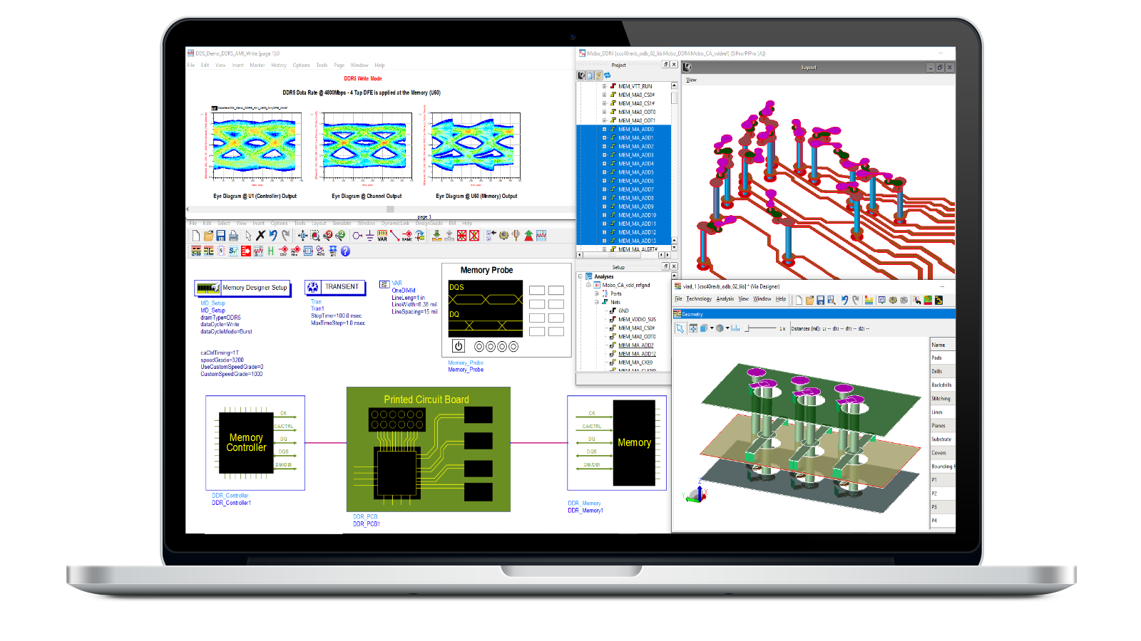
The Memory Designer improves your design productivity through smart design environment and streamlined workflows for setting up a wide range of memory interface simulations. It features state-of-the-art simulation technologies, including forwarded clocking solutions for precise jitter tracking and unmatched I/O conditions.
Highlights include:
- Supports for a wide range of memory interfaces
- Supports Keysight InfiniiMax Probe loading
- Simulation-driven compliance testing
- Crosstalk analyzer
- New Wizard driven Memory Simulation Studio (W3079E)
- Includes LPDDR5 Compliance test in the Memory Designer bundle


PCIe Design
The System Designer for PCIe® automates multi-link, multi-lane PCIe system setup with a smart design environment. The PCIe AMI Modeler quickly generates AMI models for complete system implementation, supporting both NRZ and PAM4 modulation schemes for rapid design integration. The integrated simulation-driven compliance test solution reduces design iterations and accelerates time-to-market.
Highlights include:
- Supports PCIe® Gen7 in Setup and AMI model builder
- Supports PCIe Pathfinding mode
- Supports SIPro Cell Sweep
- Integrated Seasim Interface for enhanced PCIe simulation
- Compliance Probe for comprehensive compliance test coverage
- Supports Infiniium/Infiniium 2026 Interface for advanced measurement
PCI-SIG®, PCIe® and PCI Express® are US registered trademarks and/or service marks of PCI-SIG.
USB Design
System Designer for USB is a modern and smart USB design environment for modeling and simulating the latest USB4® Gen2, Gen3 and Gen4 systems. It enables designers to perform complete USB system analysis and simulation-driven virtual compliance tests with a streamlined workflow.
Highlights include:
- Supports USB Pathfinding mode
- Supports Signal Integrity EM Professional (SIPro) Cell Sweep
- USB AMI model Builder
- Simulation-driven compliance test solution for USB – USB4® v1 and v2
- Supports Infiniium/Infiniium 2026 Interface for advanced measurement
USB Type-C®, USB-C® and USB4® are trademarks of the USB Implementers Forum


Ethernet Design
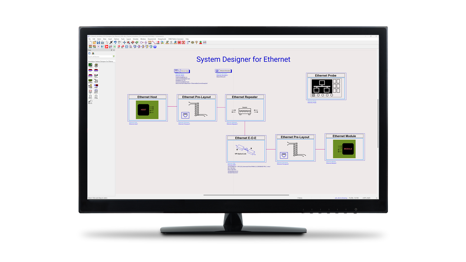
The System Designer for Ethernet streamlines the configuration of complex Ethernet systems, including multi-link, multi-lane, and PAM4 signaling, through an intelligent designenvironment. With an integrated Ethernet AMI modeler, engineers can start simulations immediately, without waiting for AMI models from silicon vendors. The built-in COM (Channel Operating Margin) interface enables validation against industry standards, and accelerates the design-to-market process, all within a unified design environment.
New features include:
- ADS Native Ethernet Compliance for IEEE802.3dj specification
- Supports COM 4.11.0
- Supports FlexDCA interface for TDECQ measurement
- Supports Infiniium/Infiniium 2026 Interface for advanced measurement
MIPI Design
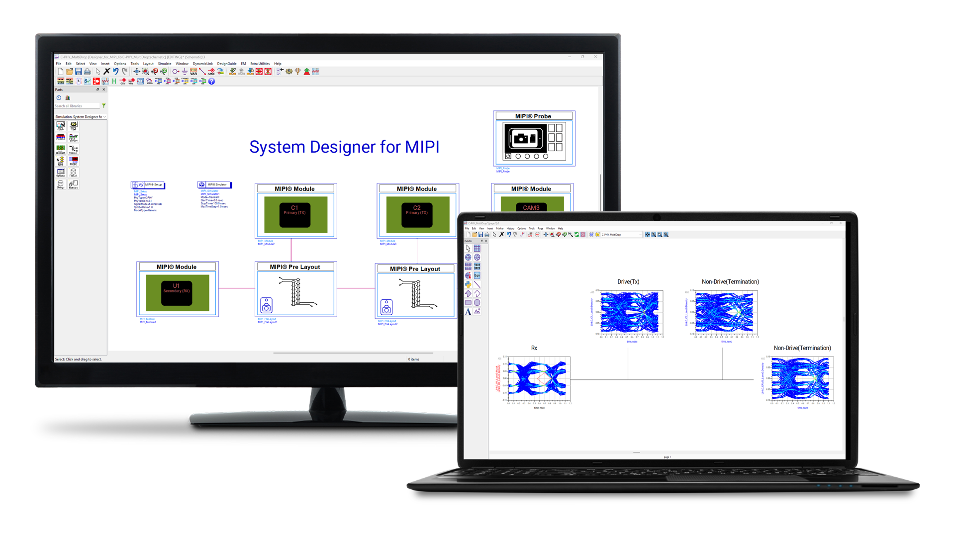
The System Designer for MIPI® simplifies the design and simulation of MIPI interfaces within a unified workflow. It supports the latest MIPI standards, including M-PHY® and C-PHY™, enabling engineers to evaluate system performance early in the design cycle. The solution automates channel setup, signal integrity analysis, and AMI model generation, helping reduce design complexity and development time. Automated setup and standards-aware configuration help engineers quickly build and evaluate complex topologies. The solution reduces validation effort while improving confidence in first-pass design success.
Highlights include:
- Supports the latest MIPI standards: M-PHY 6.0 and C-PHY 2.1.
- Performs end-to-end signal integrity analysis.
- Includes advanced C-PHY waveform source model for more realistic transmitter behavior
- Supports Multipoint Topology
- Supports MIPI M-PHY AMI Model Builder
MIPI®, M-PHY® are registered trademarks of MIPI Alliance, Inc. C-PHY™ is trademarks of MIPI Alliance, Inc. and any use of such marks by Keysight Technologies is under license. Other service marks and trade names are those of their respective owners.

SerDes Design
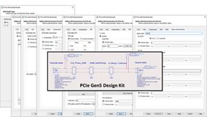
Keysight EDA’s ADS SerDes design solution offers a comprehensive design and simulation platform that effectively streamlines the SerDes design workflow, empowering designers to overcome challenges, reduce time-to-market, and refine design iterations. It covers various SerDes standards, including PCIe®, USB, Ethernet, MIPI®, and more.
Highlights include:
- MIPI® C-PHY™ waveform source Advanced TX EQ feature
- MIPI® C-PHY™ Right Eye Measurements
- USB4®V2 simulation driven compliance solutions
- PCIe® Gen5/Gen6 simulation driven compliance solutions
- Measured waveform AMI model for PAM-n
- Multi-data loading and plotting in S-Parameter toolkit
- Keysight InfiniiMax Probe Model in Smart_Eye_Probe
Signal Integrity
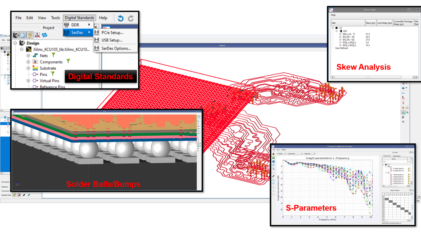
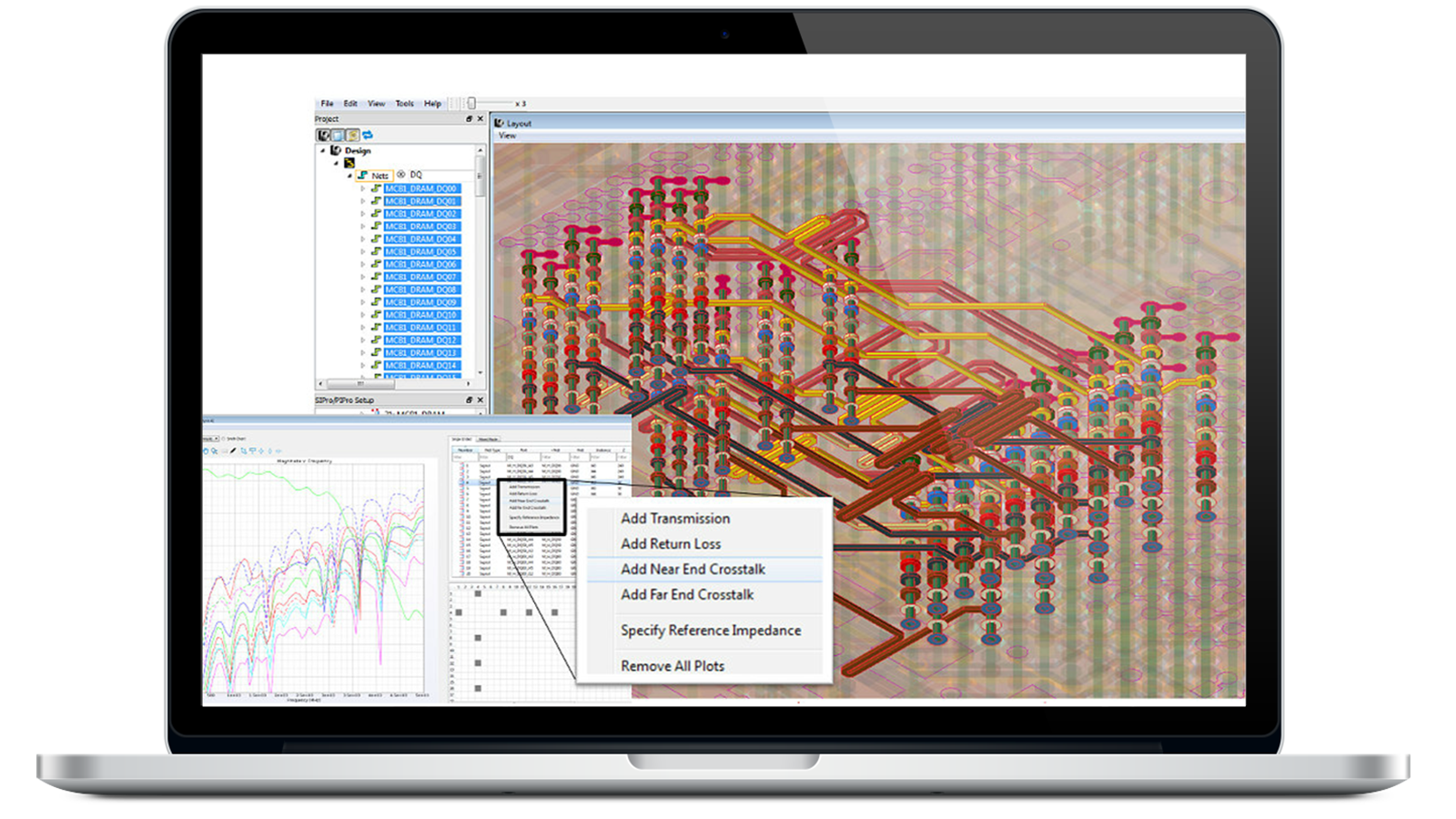
Keysight EDA's Signal Integrity EM Professional (SIPro) in ADS offers a solution for the analysis of complex high-speed PCBs and packages, enabling you to characterize loss and coupling of high-speed signal nets and extract an accurate EM model that can be used in the ADS system analysis, including Memory and SerDes applications.
Highlight includes:
- Introduction of Generation 2 simulation engine for improved accuracy
- FEM GPU support
- Silicon interposer readiness, including support for hatched grounds
- Python API, documentation and scripting improvements
- Net parametrization for rapid design exploration
- Connect LLMs using the Model Context Protocol (MCP)


Power Integrity
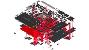
Keysight EDA's ADS with Power Integrity EM professional (PIPro) provides an integrated engineering environment for end-to-end PI ecosystem simulations. Automation makes it easy to go from PCB EM simulations for DC IR Drop, AC Impedance, and conducted EMI to a digital twin schematic for post-layout optimization and hardware debugging.
Highlights include:
- Switching VRMs and sense ports are now supported in PI-AC and PI-DS analyses
- Dynamic Sink Analysis
- Supports Multi-Phase VRM
- DC IR-Drop for Cascaded VRM
- Conducted EMI - including CISPR-25 and CISPR-32 standards
Electrical Performance Scan (EP-Scan)
The ultimate Signal Integrity and Power Integrity tool for your hardware design
Electrical Performance Scan 2026 introduces a new substrate cross-section viewer and improved layout imports. Key updates also include the addition of new specifications, improved visualization and improved stability and performance.
This video demonstrates three ways to maximize your PCB design productivity.

Design Cloud for cloud-based high-performance computing
Design Cloud
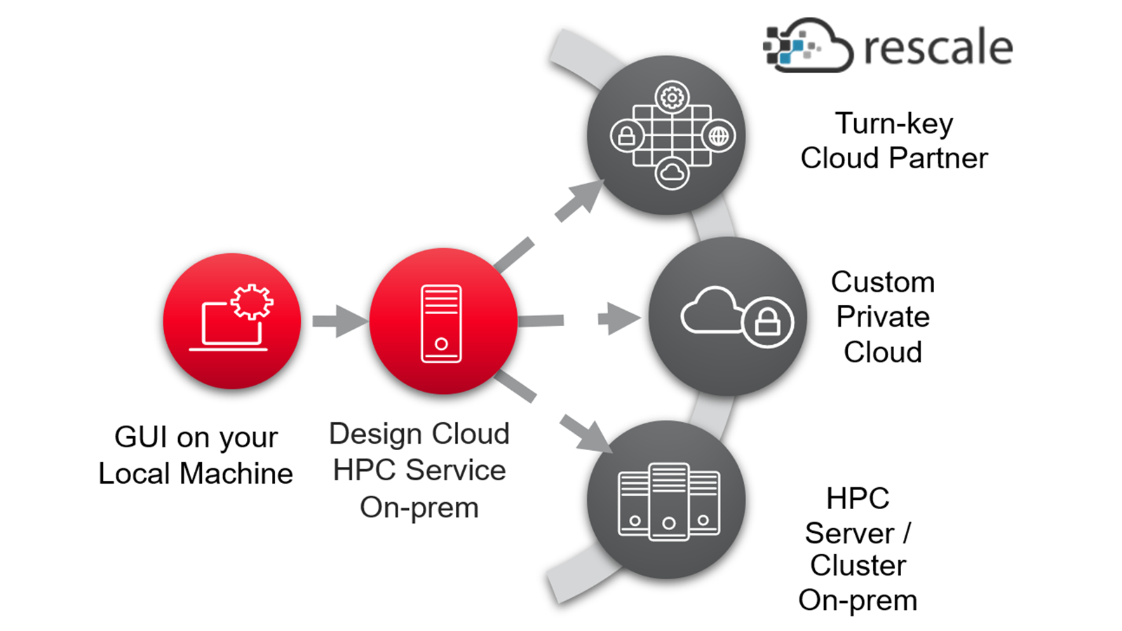
Keysight Design Cloud is a new user-experience for cloud and high-performance computing (HPC), enabling you to simulate more and wait less.
Highlights include:
- Cloud-based HPC for Memory Designer circuit and EM simulations provide parallel processing for an 80% reduction in simulation times.
- Keysight’s turn-key cloud partner, Rescale, enables you to easily launch unlimited cloud hardware in minutes.
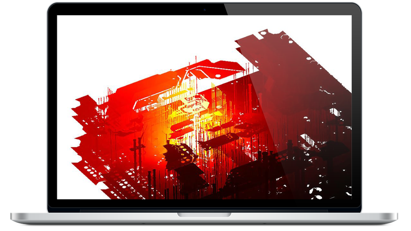
Keysight EDA Software for HSD Design



Featured Resources









Frequently Asked Questions
Electronic design is the process of creating, testing, and optimizing electronic circuits and systems. It can involve analog, digital, or mixed-signal components and technologies and applies to various domains, such as communications, data centers, and semiconductors.
EDA software is a computer-aided design category of tools for electronic circuits and systems. EDA software tools simulate the behavior and performance of electronic circuits and systems under various conditions and scenarios before fabrication or implementation. They perform different types of simulation, such as logic, functional, timing, electrical, thermal, and electromagnetic, helping designers reduce the risk of design errors, improve the quality of the final product, and save time and money in the development process.
High-speed digital design is a subset of electronic design that deals with the physical layer of digital circuits and communication systems operating at high data rates. It requires special attention to the effects of signal integrity, power integrity, electromagnetic interference, and thermal management. High-speed digital design can enable faster data transfer, lower power consumption, and higher performance in electronic systems.
Standards-driven design is an electronic design method that follows predefined specifications and protocols for communication, data exchange, and interoperability between different devices and systems. Standards-based design can facilitate compatibility, reliability, and scalability in electronic systems. Examples of standards-based design include USB, PCIe®, UCIe, and DDR.
Universal Serial Bus (USB) is a standard for communication and power delivery between devices and hosts, such as computers, smartphones, cameras, and peripherals. USB supports various data rates, from 1.5 Mbps (USB 1.0) to 80 Gbps (USB4 Version 2.0). USB also supports different power delivery modes, from 2.5 W (USB 2.0) to 240 W (USB PD 3.1). USB4 Version 2.0 is the latest version of the standard and is backward compatible with USB 3.2, USB 2.0, and Thunderbolt 3.
Peripheral Component Interconnect Express (PCIe) is a standard for high-speed serial communication between devices and hosts, such as computers, graphics cards, network cards, and storage devices. PCIe supports various data rates, from 2.5 GT/s (PCIe 1.0) to 64 GT/s (PCIe 6.0). The PCI Special Interest Group (PCI-SIG®) defines specifications and compliance tests that guarantee the interoperability of PCIe systems. PCIe also supports different lane configurations, from x1 to x32, to increase bandwidth and performance.
Universal Chiplet Interconnect Express (UCIe) is a standard for high-speed serial communication between chiplets. Designers can combine these small integrated circuits to form larger, more complex chips. UCIe is based on CXL / PCIe and supports the same data rates and lane configurations. UCIe enables chiplet-based designs that reduce cost, power consumption, and design complexity while increasing performance and scalability.
A chiplet is a small, modular chip that performs a specific function very well. For example, a chiplet can be a processor core, a memory block, an I/O driver, or a signal processing unit. Chiplets are designed to be used in a chiplet-based architecture, in which multiple chiplets are connected through a standardized high-speed digital interface, such as UCIe, to form a complete system-on-chip (SoC).
Double Data Rate (DDR) Synchronous Dynamic Random Access Memory (SDRAM) is a standard for high-speed memory communication between devices and hosts, such as computers, memory modules, and graphics cards. DDR supports various data rates, from 200 Mbps (DDR) to 6400 Mbps (DDR5). DDR also supports different memory capacities, from 64 MB (DDR) to 64 GB (DDR5). DDR transfers data on the clock signal's rising and falling edges, doubling the effective bandwidth.