How to Enhance ICT Coverage with Boundary Scan

Expand PCB Test Coverage
In-circuit testing (ICT) identifies electrical defects such as shorts and opens by probing physical test points on a printed circuit board (PCB). Boundary-scan testing, based on IEEE 1149.x standards, enables access to digital interconnections and internal nodes of integrated circuits without requiring physical probes. Combining these methods allows test engineers to validate both accessible and inaccessible nodes within complex PCB designs.
The integrated test process requires a manufacturing environment capable of coordinating ICT and boundary-scan execution within a unified system. The setup requires integration between the ICT system, boundary-scan instrumentation, automated sequencing software, and the device under test to ensure synchronized execution, stable signal integrity, and consistent fault coverage across complex PCB assemblies.


Integrated Boundary-Scan ICT Solution
Integrating boundary scan testing into manufacturing test operations requires coordinating the in-circuit test system, boundary scan analyzer, and automated test software to improve fault detection coverage across PCB assemblies. The Keysight i7090 in-line in-circuit test system integrates the x1149 boundary scan analyzer, Dynamic Link Library (DLL) connectivity, and Open Test Automation Platform (OpenTAP) software to execute boundary scan routines and electrical defect validation within a unified manufacturing test environment.
The system enables the test controller to initiate boundary scan execution and coordinate communication between the boundary scan analyzer and device under test. This ensures that boundary-scan routines are executed together with in-circuit tests within a synchronized manufacturing test process. By integrating automated test sequencing, digital interconnect validation, and in-system programming capabilities, the solution improves fault coverage, diagnostic resolution, repeatability, and manufacturing test efficiency for complex PCB assemblies.
See Block Diagram of Integrated Boundary-Scan ICT Solution


Explore Products for Our Integrated Boundary-Scan ICT Solution
-

![]()
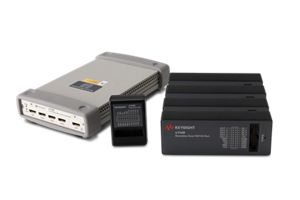
x1149 Boundary Scan Analyzer
-
![]()
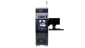
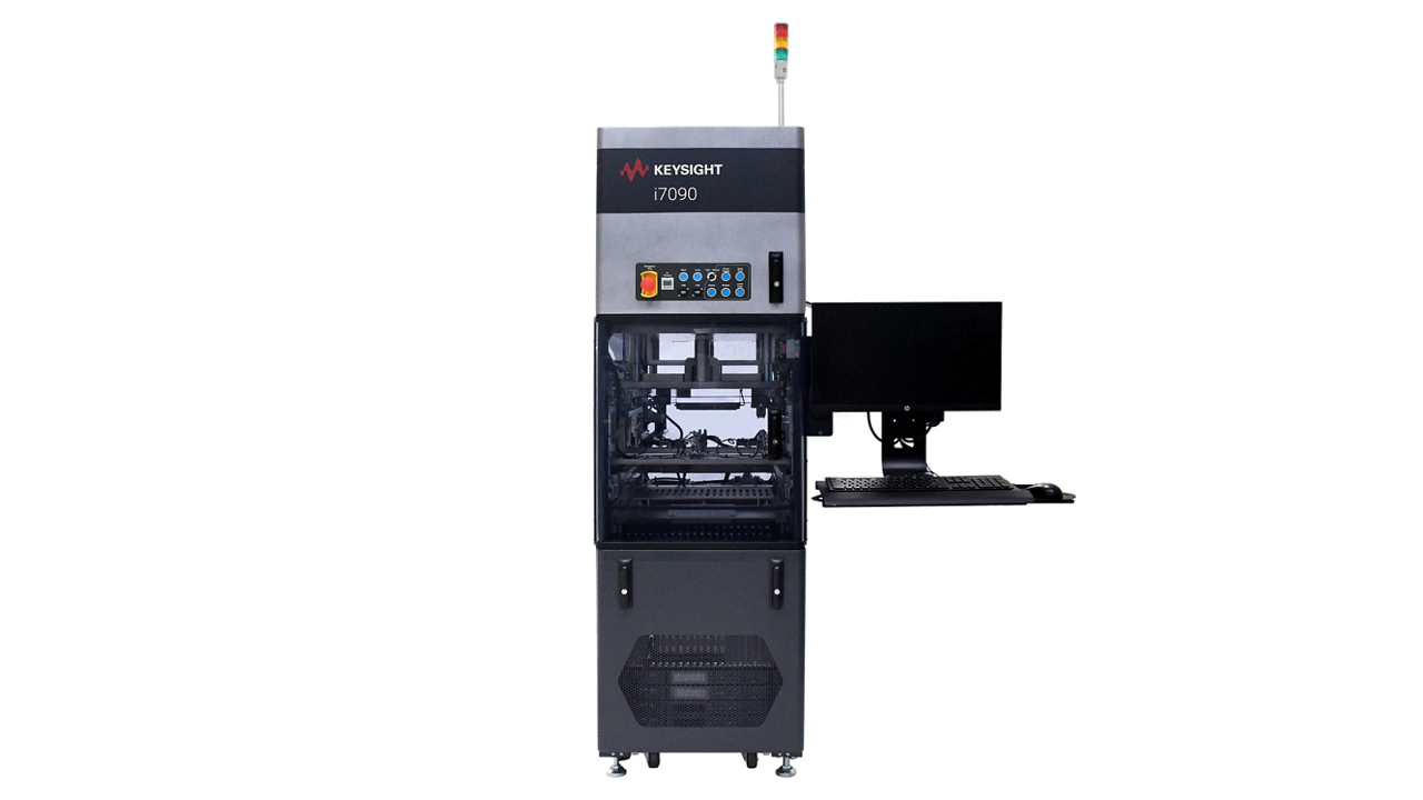
i7090 Massively Parallel and Scalable Board Test System


Discover Resources and Insights
Additional Resources for Integrated Boundary Scan ICT
Related Use Cases

-
![]()
Learn More
How to Test High-Speed PCB Assemblies
Maintain ICT coverage in high-speed PCB designs using boundary scan and limited-access test techniques.
Learn More

-
![]()
Learn More
How to Integrate In-System Programming
Integrate in-system programming into in-circuit test workflows using OpenTAP automation and functional port connectivity for PCB manufacturing test systems.
Learn More
-
![]()
Learn More
How to Verify ICT Fixture Integrity
Verify in-circuit test fixtures by detecting wiring, probe, and connectivity faults before production using automated validation tests.
Learn More

Get in Touch with One of Our Experts
Need help finding the right solution for you?