Here's the page we think you wanted. See search results instead:

Choose a country or area to see content specific to your location

    Enable browser cookies for improved site capabilities and performance.
    Keysight Technologies
    Toggle Menu
    Chat Live
    Contact Us
    Login Welcome Login

    Welcome

    • My Profile
    • Logout
    • Login
    • Register
    Quote
    United States

    Confirm Your Country or Area

    United States

    • 中国
    • 日本
    • 繁體中文
    • 한국
    • Brasil
    • Canada
    • Deutschland
    • France
    • India
    • Malaysia
    • United Kingdom
    • United States
    • Australia
    • Austria
    • Belgium
    • Denmark
    • Finland
    • Hong Kong, China
    • Ireland
    • Israel
    • Italy
    • Mexico
    • Netherlands
    • Singapore
    • Spain
    • Sweden
    • Switzerland (German)
    • Thailand
    • more...

    Please Confirm

    Confirm your country to access relevant pricing, special offers, events, and contact information.

    • PRODUCTS AND SERVICES
      • Oscilloscopes Oscilloscopes
        • Real-Time Oscilloscopes — General Purpose
        • Real-Time Oscilloscopes — Compliance
        • Equivalent-Time Sampling Oscilloscopes
        • Handheld, Modular, and USB Oscilloscopes
        • Oscilloscope Software
        • Oscilloscope Probes
        • All Oscilloscopes  
      • Analyzers Analyzers
        • Spectrum Analyzers (Signal Analyzers)
        • Network Analyzers
        • Logic Analyzers
        • Protocol Analyzers and Exercisers
        • Bit Error Ratio Testers
        • Noise Figure Analyzers and Noise Sources
        • High-Speed Digitizers and Multichannel DAQ Solutions
        • AC Power Analyzers
        • DC Power Analyzers
        • Materials Test Equipment
        • Device Current Waveform Analyzers
        • Parameter / Device Analyzers and Curve Tracers
      • Meters Meters
        • Digital Multimeter
        • Phase Noise Measurement
        • Power Meters and Power Sensors
        • Counters
        • LCR Meters and Impedance Measurement Products
        • Picoammeters and Electrometers
      • Generators, Sources, and Power Supplies Generators, Sources, and Power Supplies
        • Signal Generators (Signal Sources)
        • Waveform and Function Generators
        • Arbitrary Waveform Generators
        • Pulse Generator Products
        • HEV / EV / Grid Emulators and Test Systems
        • DC Power Supplies
        • Source / Measure Units
        • DC Electronic Loads
        • AC Power Sources
      • Software Software
        • Application Software
        • Application Software Testing
        • EDA Software
        • Test Automation Software
        • Instrument Control and Connectivity Software
        • Software Enterprise Agreement
        • All Design and Test Software  
      • Wireless Wireless
        • Wireless Network Emulators
        • Channel Emulation Solutions
        • Nemo Wireless Network Solutions
        • 5G OTA Chambers
        • Wireless Analyzers
        • IoT Regulatory Compliance Solutions
      • Modular Instruments Modular Instruments
        • PXI Products
        • AXIe Products
        • Data Acquisition System (DAQ)
        • USB Products
        • VXI Products
        • Reference Solutions
        • All Modular Instruments  
      • Network Test and Security Network Test and Security
        • Protocol and Load Test
        • Network Test Hardware
        • Cloud Test
        • Performance Monitoring
        • 5G NR Base Station Test
        • Radio Access and Core Network Test
        • Network Security Test
        • Cyber Training Simulator
        • Network Modeling
        • Application and Threat Intelligence
        • All Network Test and Security  
      • Network Visibility Network Visibility
        • Network Packet Brokers
        • Cloud Visibility
        • Network Taps | Keysight
        • Bypass Switches
        • Clock Synchronization
        • All Network Visibility  
      • Services Services
        • KeysightCare Service and Support
        • KeysightAccess Service
        • Calibration Services
        • Repair Services
        • Technology Refresh Services
        • Test as a Service — TaaS
        • Network / Security Services
        • Consulting Services
        • Financial Services
        • Education Services
        • Keysight Support Portal
        • Used Equipment
        • All Services  
      • Additional Products Additional Products
        • In-Circuit Test Systems
        • Application-Specific Test Systems and Components
        • Parametric Test Solutions
        • Photonic Test and Measurement Products
        • Laser Interferometers and Calibration Systems
        • Monolithic Laser Combiners and Precision Optics
        • MMIC Millimeter-Wave and Microwave Devices
      • All Products, Software, Services  
    • Solutions
        Explore by Use Case Explore by Industry See All Use Cases
      • All Solutions  
      • Aerospace and Defense Aerospace and Defense
      • Automotive and Energy Automotive and Energy
      • 5G 5G
      • Semiconductor Semiconductor
      • Service Providers Service Providers
      • All Industries  
    • Insights
      • Discover Insights Discover Insights
      • Success Stories Success Stories
      • Blog Blog
      • Keysight University Keysight University
      • All Insights  
    • Resources
    • Buy
    • Support
      • Keysight Product Support Keysight Product Support
      • Ixia Product Support Ixia Product Support
      • All Support  
    Welcome |
    Exit Procurement Session
    • View and Transfer Cart
    • Discard Cart and End Procurement Session

    What are you looking for?

    M9484C VXG Radar Scene Emulator AresONE-S 400GE Explore products Find a solution Get technical support Take a class Find us at events Premium used equipment KeysightCare Buy online
    Suggested searches
    No product matches found - System Exception
    Matched content
    • Home
    • Products and Services
    • W2324EP High Capacity Layout Pre-processor Element [Discontinued]

    W2324EP High Capacity Layout Pre-processor Element

    Product Status:
    Discontinued / Currently Supported
    Discontinued / Currently Supported
    Technical Support
    Technical Support
    pdf Download Data Sheet
    Prev
    Replacement Product
    W3010E PathWave ADS Layout
    View Product Details
    |
    Buy or Rent Options
    Next
    • Overview and Features
    • Post-Purchase Upgrades
    • Resources

    HIGHLIGHTS

    Note: With the enhancement to native ODB++ import and EM setup in ADS Layout in ADS 2015.01, W2324 High capacity layout pre-processor is being phased out because its capabilities are superseded by this most recent version of ADS Layout.

    • Last day for a quote: March 31, 2015
    • Last day to order perpetual and TBLs: July 31, 2015
    • Last day to order support: July 31, 2016

    The Advanced Design System (ADS) High Capacity Layout Pre-processor Element includes the following capabilities when used in a high-speed digital design flow:

    • Imports large PCB design files in ODB++ format into a pre-processor GUI
    • Allows critical net selection and cookie cutting
    • Exports processed segment of PCB to ADS Layout for EM modeling using Momentum and FEM Element
    • Supports import of netnames and components

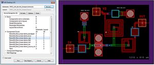
    The High Capacity Layout Pre-processor Element is an ODB++ file format import and pre-processing tool that enables you select the environment immediately around critical nets in preparation for electromagnetic (EM) modeling. This type of pre-processing is useful in high-speed digital design where the printed circuit board (PCB) is very complex and whose total geometry exceeds the capacity of an EM-based field solver. The solution is to focus in on a handful of critical nets; for example, a differential pair connecting two Serializer/Deserializer (SERDES) integrated circuits (ICs) that is a victim of crosstalk from one or more aggressor traces. An example of such a trace is shown highlighted below in Figure 1. Note that the board has been “cookie cut” meaning a convex hull with a user-defined margin has been defined, leaving a portion of the board whose complexity is within the capacity constraints of full-accuracy, full-wave EM field solvers such as Momentum and FEM Element.

    Critial Nets

    Figure 1. One of several critical nets is highlighted in cyan. Note that this very large PCB has been “cookie cut,” with the left hand edge being a convex hull that includes this leftmost net and a margin around it.

    A typical high-speed digital workflow including High Capacity Layout Pre-processor Element in shown in Figure 2 below.

    High Speed Digital Design Flow

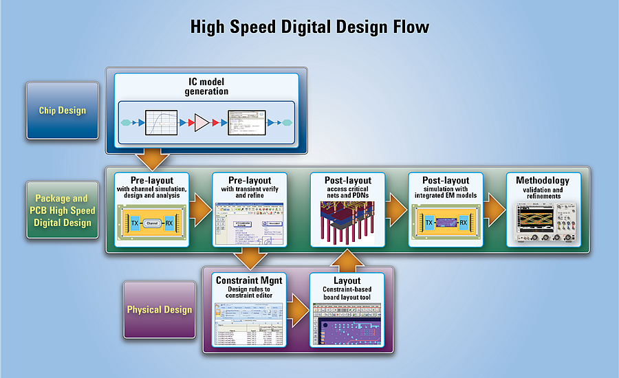
    Figure 2. The High Capacity Layout Pre-processor is central to this high-speed digital design flow. The middle bar (green) and lower bar (purple) encloses steps performed by the signal integrity engineer in ADS, and by the physical designer in the third-party enterprise PCB tool, respectively. The task in the upper (blue) bar is performed by the chip designer.

    First, the signal integrity engineer combines vendor IC models with a pre-layout “placeholder” for the channel. Typically this placeholder is created from the ADS Multi-Layer Models (MLM) transmission line library possibly supplemented with EM-based via models. The goal of the pre-layout simulation batches is to explore the design space and optimize IC settings (such as the transmitter (Tx) SERDES pre-emphasis filter taps and the receiver (Rx) SERDES equalizer taps and clock/data recovery (CDR) circuit settings), stack up, controlled impedance line geometry, and via design.

    These parameters are given to the physical designer to load into the Constraint Editor of the auto-router of a third-party enterprise PCB tool such as Expedition from Mentor Graphics. Once the board is routed, post-layout artwork is available in ODB++ file format.

    The signal integrity engineer selects the critical nets and pre-processes the important section of the PCB for EM modeling. The resulting EM model is used to “swap out” the pre-layout placeholder with the characteristics of the actual post-layout design. In this way the candidate layout can be verified before manufacturing. If the candidate design has issues such as excessive crosstalk, the signal integrity engineer can adjust the critical area in the ADS Layout “sandbox” (for example by added stitching vias or guard traces) and solve the new candidate until a satisfactory adjustment is proven in. The physical designer then applies the knowledge from the ADS experimentation to the “golden” copy of the design in the third-party enterprise PCB tool for first pass success. This methodology avoids the expensive, time consuming, and non-deterministic “cut and try” approach to qualifying the post-layout, namely serial fabrication and measurement of multiple prototypes.

    Learn more about Advanced Design System (ADS) Simulation Elements

    Sort by :
    Date
    Date Title
    Filter Results
    No information found for this product
    Reset
    By Type of Content
    Back to Top

    Explore

    • Products + Services
    • Solutions
    • Industries
    • Events
    • Keysight University

    Insights

    • Discover Insights
    • Success Stories
    • Resources
    • Blog
    • Community

    Partners

    Support

    • Keysight Product Support
    • Ixia Product Support
    • Manage Software Licenses
    • Product Order Status
    • Parts

    About Keysight

    • Newsroom
    • Investor Relations
    • Quality and Security
    • Corporate Social Responsibility
    • Diversity, Equity, and Inclusion
    • Modern Slavery Act Transparency Statement
    • Careers

    • Facebook: Connect with Keysight LinkedIn: Connect with Keysight Twitter: Connect with Keysight YouTube: Connect with Keysight WeChat:Connect with Keysight
    • © Keysight Technologies 2000–2023
    • Privacy
    • Sitemap
    • Terms
    • Trademark Acknowledgements
    • Feedback