Learn More
segmentation:campaign/Digital_High_Performance,segmentation:product-category/Oscilloscopes_BERTs_AWGs,segmentation:product-category/Oscilloscopes_BERTs_AWGs/Oscilloscopes_2GHz_higher,segmentation:business-unit/CSG,keysight:product-lines/1a,segmentation:funnel/bofu,keysight:dtx/solutions/facets/design-and-test-product/oscilloscope---logic-analyzer,keysight:dtx/solutions/facets/workflow-stage/qa,keysight:dtx/solutions/facets/development-area/high-speed-digital,keysight:dtx/solutions/facets/industry/semiconductor,keysight:dtx/solutions/facets/industry/wireline-communications,keysight:models/ux/uxr0594bsegmentation:campaign/Digital_High_Performance,segmentation:product-category/Oscilloscopes_BERTs_AWGs,segmentation:product-category/Oscilloscopes_BERTs_AWGs/Oscilloscopes_2GHz_higher,segmentation:business-unit/CSG,keysight:product-lines/1a,segmentation:funnel/bofu,keysight:dtx/solutions/facets/design-and-test-product/oscilloscope---logic-analyzer,keysight:dtx/solutions/facets/workflow-stage/qa,keysight:dtx/solutions/facets/development-area/high-speed-digital,keysight:dtx/solutions/facets/industry/semiconductor,keysight:dtx/solutions/facets/industry/wireline-communications,keysight:models/ux/uxr0594bsegmentation:campaign/Digital_High_Performance,segmentation:product-category/Oscilloscopes_BERTs_AWGs,segmentation:product-category/Oscilloscopes_BERTs_AWGs/Oscilloscopes_2GHz_higher,segmentation:business-unit/CSG,keysight:product-lines/1a,segmentation:funnel/bofu,keysight:dtx/solutions/facets/design-and-test-product/oscilloscope---logic-analyzer,keysight:dtx/solutions/facets/workflow-stage/qa,keysight:dtx/solutions/facets/development-area/high-speed-digital,keysight:dtx/solutions/facets/industry/semiconductor,keysight:dtx/solutions/facets/industry/wireline-communications,keysight:models/ux/uxr0594bsegmentation:campaign/Digital_High_Performance,segmentation:product-category/Oscilloscopes_BERTs_AWGs,segmentation:product-category/Oscilloscopes_BERTs_AWGs/Oscilloscopes_2GHz_higher,segmentation:business-unit/CSG,keysight:product-lines/1a,segmentation:funnel/bofu,keysight:dtx/solutions/facets/design-and-test-product/oscilloscope---logic-analyzer,keysight:dtx/solutions/facets/workflow-stage/qa,keysight:dtx/solutions/facets/development-area/high-speed-digital,keysight:dtx/solutions/facets/industry/semiconductor,keysight:dtx/solutions/facets/industry/wireline-communications,keysight:models/ux/uxr0594bsegmentation:campaign/Digital_High_Performance,segmentation:product-category/Oscilloscopes_BERTs_AWGs,segmentation:product-category/Oscilloscopes_BERTs_AWGs/Oscilloscopes_2GHz_higher,segmentation:business-unit/CSG,keysight:product-lines/1a,segmentation:funnel/bofu,keysight:dtx/solutions/facets/design-and-test-product/oscilloscope---logic-analyzer,keysight:dtx/solutions/facets/workflow-stage/qa,keysight:dtx/solutions/facets/development-area/high-speed-digital,keysight:dtx/solutions/facets/industry/semiconductor,keysight:dtx/solutions/facets/industry/wireline-communications,keysight:models/ux/uxr0594bsegmentation:campaign/Digital_High_Performance,segmentation:product-category/Oscilloscopes_BERTs_AWGs,segmentation:product-category/Oscilloscopes_BERTs_AWGs/Oscilloscopes_2GHz_higher,segmentation:business-unit/CSG,keysight:product-lines/1a,segmentation:funnel/bofu,keysight:dtx/solutions/facets/design-and-test-product/oscilloscope---logic-analyzer,keysight:dtx/solutions/facets/workflow-stage/qa,keysight:dtx/solutions/facets/development-area/high-speed-digital,keysight:dtx/solutions/facets/industry/semiconductor,keysight:dtx/solutions/facets/industry/wireline-communications,keysight:models/ux/uxr0594bsegmentation:campaign/Digital_High_Performance,segmentation:product-category/Oscilloscopes_BERTs_AWGs,segmentation:product-category/Oscilloscopes_BERTs_AWGs/Oscilloscopes_2GHz_higher,segmentation:business-unit/CSG,keysight:product-lines/1a,segmentation:funnel/bofu,keysight:dtx/solutions/facets/design-and-test-product/oscilloscope---logic-analyzer,keysight:dtx/solutions/facets/workflow-stage/qa,keysight:dtx/solutions/facets/development-area/high-speed-digital,keysight:dtx/solutions/facets/industry/semiconductor,keysight:dtx/solutions/facets/industry/wireline-communications,keysight:models/ux/uxr0594bsegmentation:campaign/Digital_High_Performance,segmentation:product-category/Oscilloscopes_BERTs_AWGs,segmentation:product-category/Oscilloscopes_BERTs_AWGs/Oscilloscopes_2GHz_higher,segmentation:business-unit/CSG,keysight:product-lines/1a,segmentation:funnel/bofu,keysight:dtx/solutions/facets/design-and-test-product/oscilloscope---logic-analyzer,keysight:dtx/solutions/facets/workflow-stage/qa,keysight:dtx/solutions/facets/development-area/high-speed-digital,keysight:dtx/solutions/facets/industry/semiconductor,keysight:dtx/solutions/facets/industry/wireline-communications,keysight:models/ux/uxr0594bsegmentation:campaign/Digital_High_Performance,segmentation:product-category/Oscilloscopes_BERTs_AWGs,segmentation:product-category/Oscilloscopes_BERTs_AWGs/Oscilloscopes_2GHz_higher,segmentation:business-unit/CSG,keysight:product-lines/1a,segmentation:funnel/bofu,keysight:dtx/solutions/facets/design-and-test-product/oscilloscope---logic-analyzer,keysight:dtx/solutions/facets/workflow-stage/qa,keysight:dtx/solutions/facets/development-area/high-speed-digital,keysight:dtx/solutions/facets/industry/semiconductor,keysight:dtx/solutions/facets/industry/wireline-communications,keysight:models/ux/uxr0594bsegmentation:campaign/Digital_High_Performance,segmentation:product-category/Oscilloscopes_BERTs_AWGs,segmentation:product-category/Oscilloscopes_BERTs_AWGs/Oscilloscopes_2GHz_higher,segmentation:business-unit/CSG,keysight:product-lines/1a,segmentation:funnel/bofu,keysight:dtx/solutions/facets/design-and-test-product/oscilloscope---logic-analyzer,keysight:dtx/solutions/facets/workflow-stage/qa,keysight:dtx/solutions/facets/development-area/high-speed-digital,keysight:dtx/solutions/facets/industry/semiconductor,keysight:dtx/solutions/facets/industry/wireline-communications,keysight:models/ux/uxr0594bsegmentation:campaign/Digital_High_Performance,segmentation:product-category/Oscilloscopes_BERTs_AWGs,segmentation:product-category/Oscilloscopes_BERTs_AWGs/Oscilloscopes_2GHz_higher,segmentation:business-unit/CSG,keysight:product-lines/1a,segmentation:funnel/bofu,keysight:dtx/solutions/facets/design-and-test-product/oscilloscope---logic-analyzer,keysight:dtx/solutions/facets/workflow-stage/qa,keysight:dtx/solutions/facets/development-area/high-speed-digital,keysight:dtx/solutions/facets/industry/semiconductor,keysight:dtx/solutions/facets/industry/wireline-communications,keysight:models/ux/uxr0594bsegmentation:campaign/Digital_High_Performance,segmentation:product-category/Oscilloscopes_BERTs_AWGs,segmentation:product-category/Oscilloscopes_BERTs_AWGs/Oscilloscopes_2GHz_higher,segmentation:business-unit/CSG,keysight:product-lines/1a,segmentation:funnel/bofu,keysight:dtx/solutions/facets/design-and-test-product/oscilloscope---logic-analyzer,keysight:dtx/solutions/facets/workflow-stage/qa,keysight:dtx/solutions/facets/development-area/high-speed-digital,keysight:dtx/solutions/facets/industry/semiconductor,keysight:dtx/solutions/facets/industry/wireline-communications,keysight:models/ux/uxr0594b
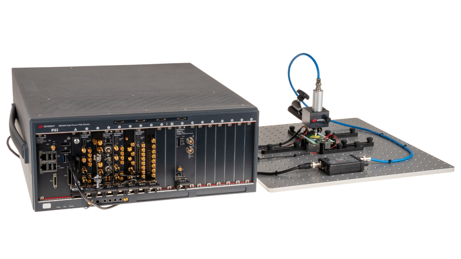
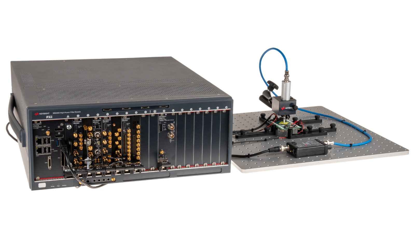
How to Measure GDDR7 PAM Eye Diagrams
Measure GDDR7 PAM eye diagrams with jitter, noise, and margin analysis using oscilloscope-based validation workflows.
Learn More