What are you looking for?
High-Speed Digital Suite
Have confidence in your PCB designs before build-out
Designers need agility to handle today’s denser and more complex designs. Keysight EDA’s Advanced Design System (ADS) streamlines design verification and compliance through guided collaboration and standard-driven workflows.
Advanced packaging workflows
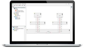

Streamlined Chiplet and 3DIC Advanced Package Designs
Chiplet adoption is accelerating across AI, HPC, data center, networking, and automotive systems as designers move beyond monolithic scaling. But multi-die architectures introduce new challenges: complex interconnect structures, silicon interposers and bridges, hatched ground planes, and high-speed die-to-die standards such as UCIe and BoW.
Keysight’s Chiplet and 3DIC Interconnect Design solutions help engineers model, design, and validate advanced package interconnects earlier in the design flow, reducing risk and accelerating development.
Standards-Driven Workflows
DDR 5/LPDDR6 model extraction, signal integrity, and compliance verification
The ADS Memory Designer minimizes the effort required to generate IBIS-AMI models for receivers, extract accurate DDR channel electromagnetic (EM) models, and predict the margin to the eye mask at specific bit error rates.
Built-in support for the latest memory standards, DDR5 and LPDDR6, and advanced signal integrity analysis capabilities with unwavering accuracy allow designers to set up end-to-end DDR analysis five times faster than before.
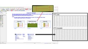

Chiplet die-to-die link signal integrity, and compliance verification
The ADS Chiplet PHY designer allows designers to predict the end-to-end link margin and compliance measures such as VTF for chiplet’s die-to-die interconnects.
It enables the forwarded clocking in UCIe to be accurately analyzed to consider the jitter tracking. Built-in support for standard-specific measurements makes verifying compliance with known chiplet standards easy.
PCIe® 5/6/7 signal integrity, and virtual compliance test
The ADS System Designer for PCIe® automates the setup for multi-link, multi-lane, and multi-level (PAM4) PCIe systems using a smart design environment. The PCIe AMI modeler, which supports NRZ and PAM4 modulations, facilitates the quick implementation of PCIe systems.
The integrated simulation-driven compliance test solution can reduce design costs by minimizing design iterations and shortening time-to-market.


Streamline USB Design and Compliance
The ADS System Designer for USB makes it easier to design and validate high-performance USB systems, including USB4®. It automates the setup for complex multi-link and multi-lane configurations, offering a smart way to simulate USB system behavior.
The USB AMI model builder supports NRZ and PAM3 modulations, aiding in the quick implementation of spec-compliant USB transmitters and receivers. Virtual compliance testing integrated into the simulation ensures designs meet the latest requirements, reducing iterations and accelerating time to market.
Streamlined Workflow for Next-Generation Ethernet System Design
System Designer for Ethernet delivers a unified and streamlined workflow for analyzing the latest Ethernet standards, supporting data rates from 100G to 1.6Tb/s, while incorporating electrical-optical-electrical (EOE) system design for true end-to-end validation. It empowers designers to accelerate the development and validation of next-generation Ethernet systems through an intelligent design environment and advanced AMI model generation capabilities.


Signal Integrity EM Extraction Workflow
Each new digital standard brings faster speeds and higher frequencies. Signal integrity engineers need to have confidence in their channel design, including optimal via design, managing crosstalk, signal loss, jitter, and equalization.
With advanced channel simulation in ADS, you can simulate for pulsed amplitude modulation (PAM-4, PAM-3, and PAM-N) signaling schemes. Complemented by fast and accurate signal integrity EM analysis, you can achieve 100% board success by catching critical errors before build-out.
View Lessons
Designing for Signal Integrity (10 min)
Power Integrity Workflow
With lower voltages, higher currents, and multiple supplies, power integrity issues can be difficult to troubleshoot and cost thousands of dollars to fix. Overcoming this challenge requires a cohesive design flow for frequency and time-domain analysis of power distribution networks (PDNs).
With Keysight’s power integrity (PI) design workflow, you can visualize the worst-case ripple caused by a dynamic load and engineer an optimum low-noise PDN.


High-Speed Digital Design: Go Deeper
Printed circuit boards (PCBs) get more complex and densely packed as technology advances and devices shrink.
Learn more with a deeper dive into standards-driven workflows, signal and power integrity with a curated selection of advanced topics.
Protect Your Innovation Investment


Innovate at speed by ensuring up-to-date application software & firmware and expert technical support at our fastest available times.


Software licensing, terms, and types
Keysight software licensing options provide flexibility and support. Choose your terms, choose your type, and keep control of your budget.


Manage your Keysight software, view and request licenses, and get the latest software updates.
Electronic Design and High-Speed Digital Design FAQ
A guide to common questions and answers about electronic design, high-speed digital design, and standards-driven design
Electronic design is the process of creating, testing, and optimizing electronic circuits and systems. It can involve analog, digital, or mixed-signal components and technologies and applies to various domains, such as communications, data centers, and semiconductors.
EDA software is a computer-aided design category of tools for electronic circuits and systems. EDA software tools simulate the behavior and performance of electronic circuits and systems under various conditions and scenarios before fabrication or implementation. They perform different types of simulation, such as logic, functional, timing, electrical, thermal, and electromagnetic, helping designers reduce the risk of design errors, improve the quality of the final product, and save time and money in the development process.
High-speed digital design is a subset of electronic design that deals with the physical layer of digital circuits and communication systems operating at high data rates. It requires special attention to the effects of signal integrity, power integrity, electromagnetic interference, and thermal management. High-speed digital design can enable faster data transfer, lower power consumption, and higher performance in electronic systems.
Standards-driven design is an electronic design method that follows predefined specifications and protocols for communication, data exchange, and interoperability between different devices and systems. Standards-based design can facilitate compatibility, reliability, and scalability in electronic systems. Examples of standards-based design include USB, PCIe® , UCIe, and DDR.
USB is a standard for communication and power delivery between devices and hosts, such as computers, smartphones, cameras, and peripherals. USB supports various data rates, from 1.5 Mbps (USB 1.0) to 80 Gbps (USB4 Version 2.0). USB also supports different power delivery modes, from 2.5 W (USB 2.0) to 240 W (USB PD 3.1). USB4 Version 2.0 is the latest version of the standard and is backward compatible with USB 3.2, USB 2.0, and Thunderbolt 3.
PCIe is a standard for high-speed serial communication between devices and hosts, such as computers, graphics cards, network cards, and storage devices. PCIe supports various data rates, from 2.5 GT/s (PCIe 1.0) to 64 GT/s (PCIe 6.0). The PCI Special Interest Group (PCI-SIG®) defines specifications and compliance tests that guarantee the interoperability of PCIe systems. PCIe also supports different lane configurations, from x1 to x32, to increase bandwidth and performance.
Universal Chiplet Interconnect Express (UCIe) is a standard for high-speed serial communication between chiplets. Designers can combine these small integrated circuits to form larger, more complex chips. UCIe is based on CXL / PCIe and supports the same data rates and lane configurations. UCIe enables chiplet-based designs that reduce cost, power consumption, and design complexity while increasing performance and scalability.
Double Data Rate (DDR) SDRAM is a standard for high-speed memory communication between devices and hosts, such as computers, memory modules, and graphics cards. DDR supports various data rates, from 200 Mbps (DDR) to 6400 Mbps (DDR5). DDR also supports different memory capacities, from 64 MB (DDR) to 64 GB (DDR5). DDR transfers data on the clock signal's rising and falling edges, doubling the effective bandwidth.
A chiplet is a small, modular chip that performs a specific function very well. For example, a chiplet can be a processor core, a memory block, an I/O driver, or a signal processing unit. Chiplets are designed to be used in a chiplet-based architecture, in which multiple chiplets are connected through a standardized high-speed digital interface, such as UCIe, to form a complete system-on-chip (SoC).
Want help or have questions?