
HMMC-5629 DC-26.5 GHz HBT Limiting Amplifier
데이터 시트
Introduction
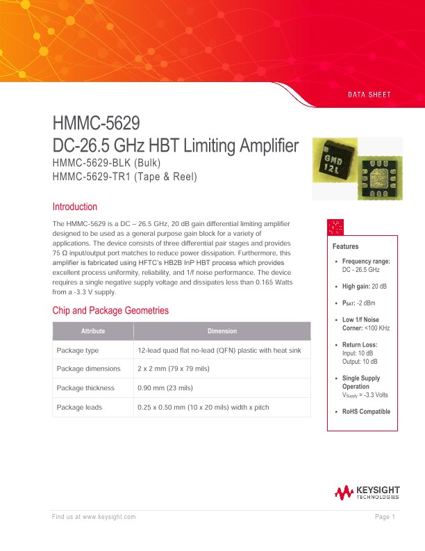
The HMMC-5629 is a DC – 26.5 GHz, 20 dB gain differential limiting amplifier designed to be used as a general purpose gain block for a variety of applications. The device consists of three differential pair stages and provides 75 Ω input/output port matches to reduce power dissipation. Furthermore, this amplifier is fabricated using HFTC’s HB2B InP HBT process which provides excellent process uniformity, reliability, and 1/f noise performance. The device requires a single negative supply voltage and dissipates less than 0.165 Watts from a -3.3 V supply.
Absolute Maximum Ratings 1
Symbol |
Parameters/Conditions |
Min. |
Max. |
Units |
Vee |
Collector Pad Voltage |
-3.5 |
|
Volts |
Iout |
Maximum Collector Current |
|
60 |
mA |
Pin |
CW Input Power |
|
5 |
dBm |
Tj |
Maximum Junction Temperature 2 |
|
150 |
°C |
TA 3 |
Ambient Temperature |
-55 |
75 |
°C |
Tstg |
Storage Temperature |
-65 |
150 |
°C |
Tmax 4 |
Maximum Assembly Temperature |
|
260 |
°C |
DC Specifications/Physical Properties 1
Symbol |
Parameters/Conditions |
Min. |
Typ. |
Max. |
Units |
Vee |
Supply Voltage |
-3.5 |
-3.3 |
-3.0 |
V |
Iee |
Supply Current |
40 |
50 |
60 |
mA |
Rcm |
Resistance from Vcm to either output |
|
5000 |
|
Ω |
Iadj |
Reference Current |
3 |
4 |
5 |
mA |
Vadj |
Voltage on Iadj pin |
-0.5 |
0 |
0.5 |
V |
Vtd |
Temperature Diode Voltage |
-0.8 |
|
0.8 |
V |
Frequency-Domain RF Specifications 1
Symbol |
Parameters/Conditions |
DC - 20 GHz |
|
DC - 20-26.5 GHz |
Units |
|||
|
|
|
|
|
|
|||
|
|
Min. |
Typ. |
Max. |
Min. |
Typ. |
Max. |
|
S21 |
Small Signal Gain |
14 |
20 |
25 |
11 |
17 |
23 |
dB |
RLin |
Input Return Loss |
5 |
10 |
|
5 |
10 |
|
dB |
RLout |
Output Return Loss |
5 |
10 |
|
5 |
10 |
|
dB |
ISO |
Reverse Isolation |
|
-65 |
-50 |
|
-60 |
-40 |
dB |
Pout |
Output Power with Pin = -15 dBm |
|
-2 |
|
|
-3.5 |
|
dBm |
NF |
Noise Figure |
|
15 |
|
|
15 |
|
dB |
Biasing
In nominal operation the HMMC-5629 is biased with a single negative 3.3 V supply applied to the Vee pin and the Iadj pin is grounded.
Additionally, if a precise output voltage is required, a precision current source can be applied to the Iadj pin. This reference current is nominally set to 4 mA and must not be less than 3 mA nor greater than 5 mA. During power-up, first set Vee to -3.3 V then set the current into the Iadj pin to 4 mA. When powering down, set Iadj to 0 mA or disconnect then turn down Vee.
The common mode output voltage can be monitored at the Vcm pin and two anti-polar temperature diodes connected between the TD pin and ground can be used to stabilize the output voltage over temperature.
Assembly Techniques
The HMMC-5629 is fabricated using an InP-based HBT semiconductor material structure which limits the maximum assembly temperature to 150°C. Due to the fact AuSn solder dieattach temperatures exceed this limit, only epoxy-based die-attach materials and processes (such as 84-1LMI) should be employed during HMMC-5629 assembly.
GaAs and InP MMICs are ESD sensitive. ESD preventive measures must be employed in all aspects of storage, handling, and assembly.
Keysight application note #54, “GaAs MMIC ESD, Die Attach, and Bonding Guidelines” provides basic information on the subjects.