Semiconductor Solutions

- Design and Simulation
- Device Modeling
- IP Management
- Wafer Test
- Device Test
Optimize semiconductor design and performance with fast, accurate multi-domain simulation solutions.
RF Circuit Design and Simulation
Accelerate RF circuit design with integrated layout, EM, and circuit simulation.
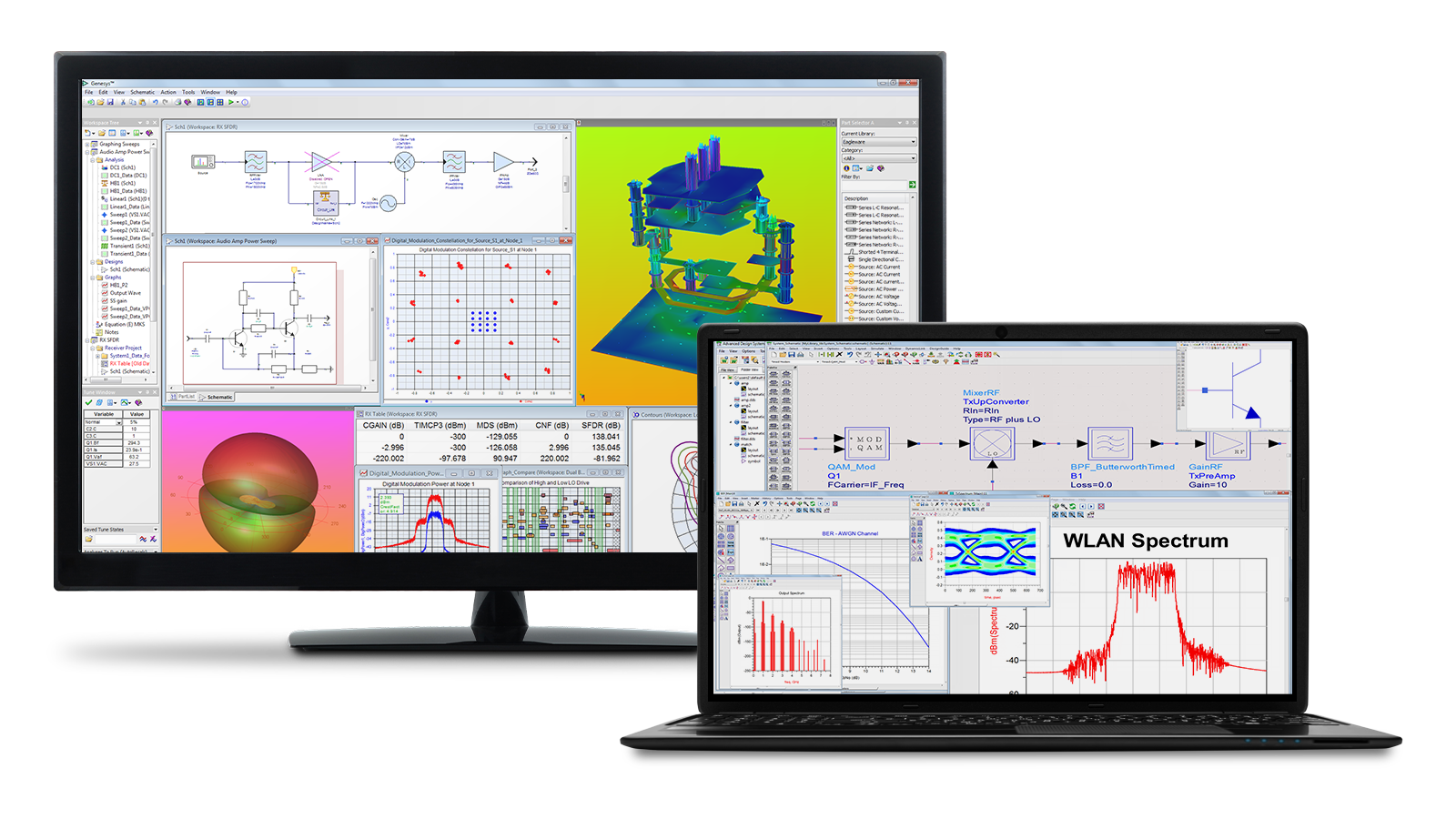
Electro-Thermal Design
Simulate coupled electrical and thermal effects to optimize semiconductor reliability and performance.
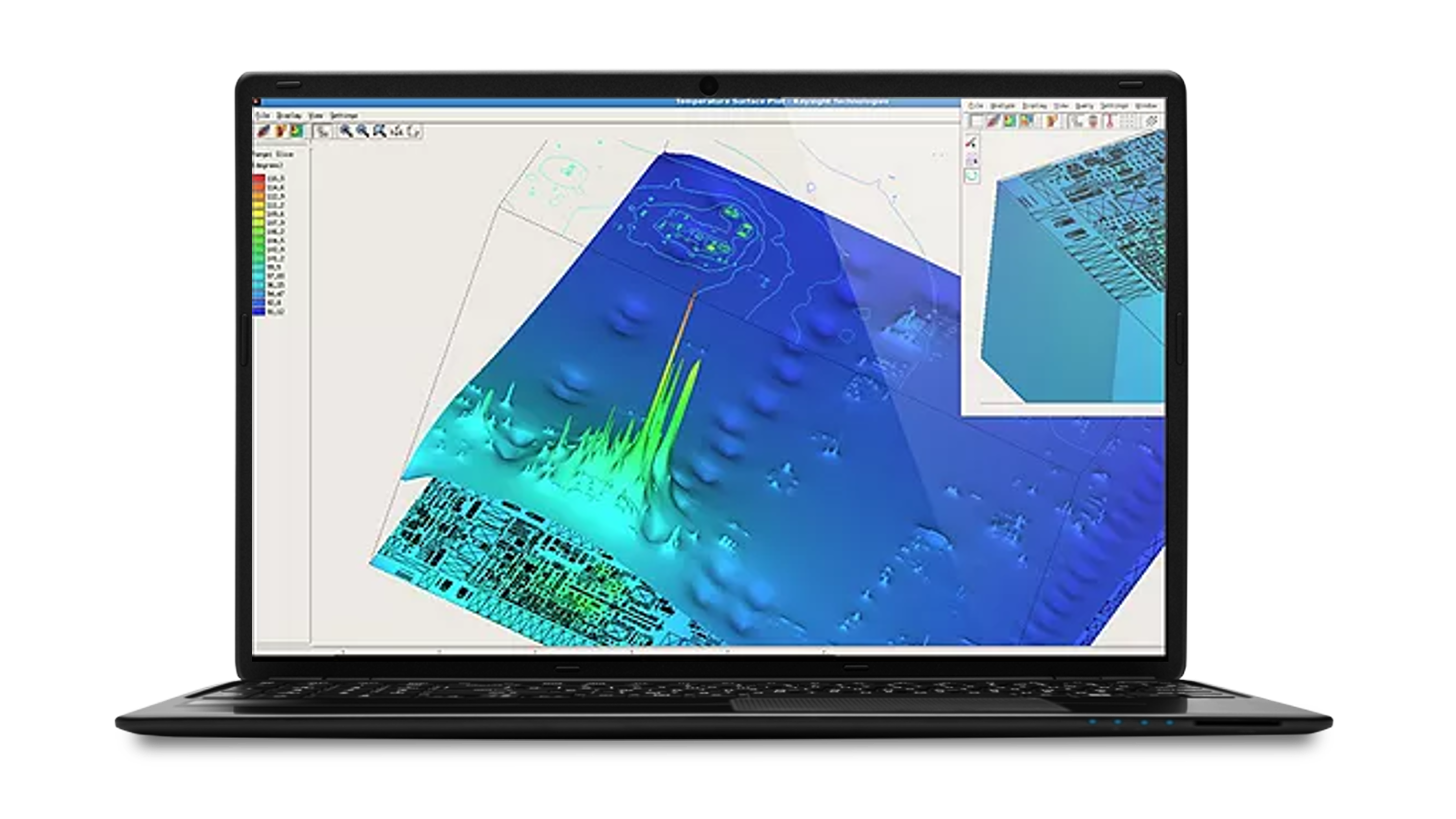
3D EM Simulation
Simulate electromagnetic effects in complex 3D semiconductor structures for accurate design validation.
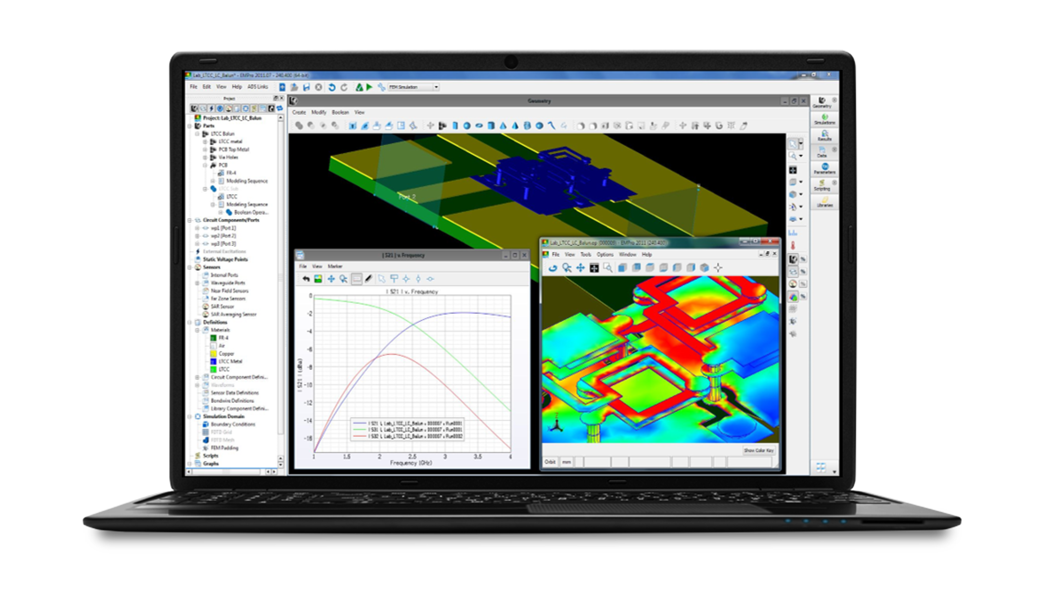
RF Synthesis
Automate RF and microwave circuit synthesis for fast, accurate semiconductor design.

Wafer Characterization Test
Streamline wafer-level measurements for semiconductor device evaluation.
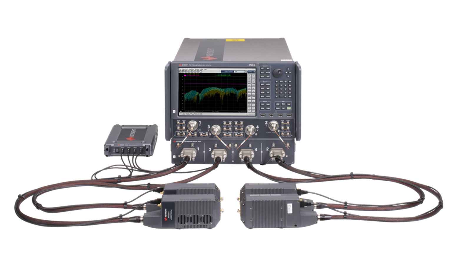
3D Heterogeneous Integration and Chiplets
Model advanced 3D heterogeneous integration and chiplet architectures with full EM accuracy.
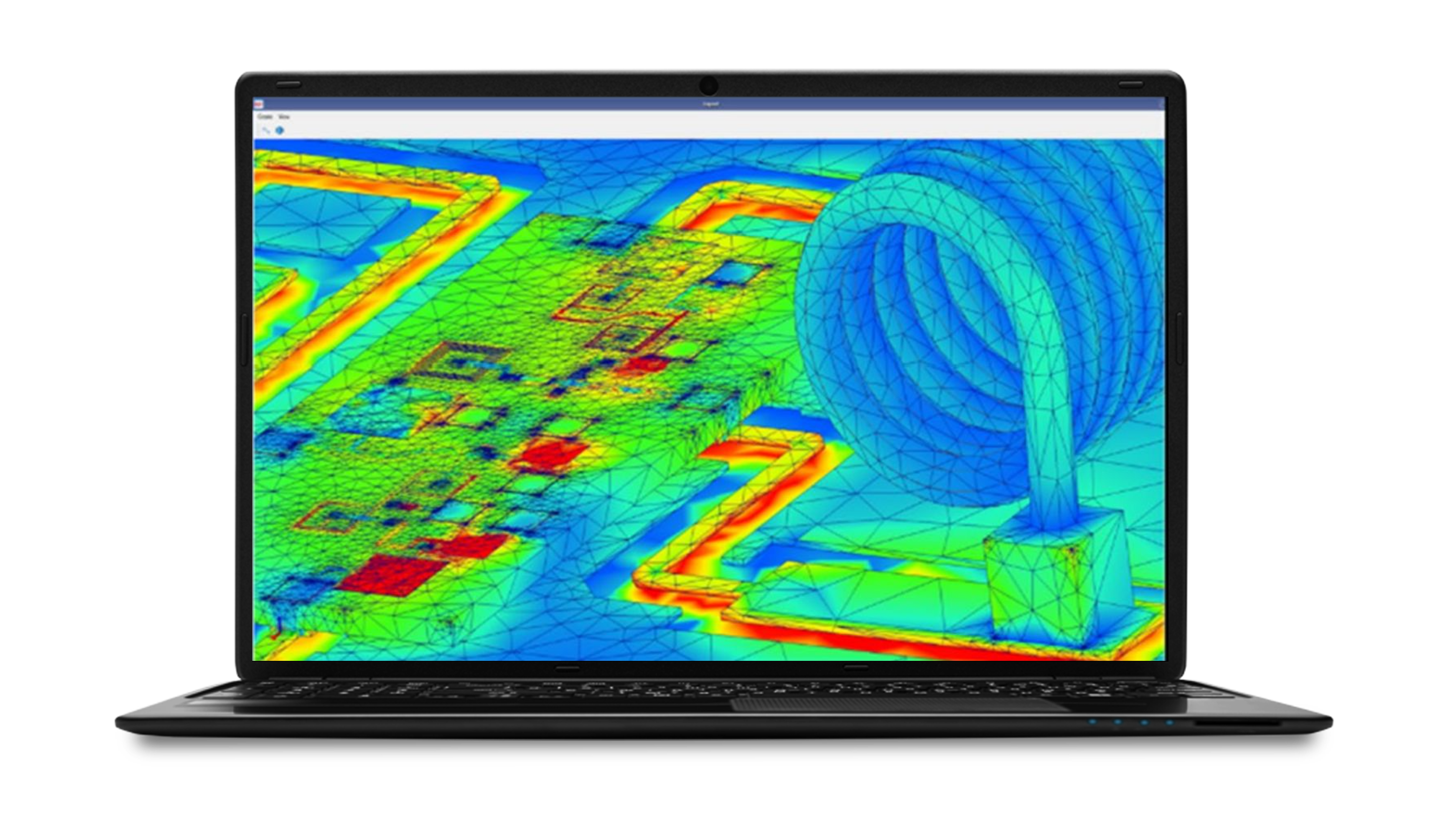
Photonic Simulation
Design and optimize photonic devices and integrated circuits for semiconductor applications.

Superconducting Quantum Circuit Simulation
Model and simulate flux-quantizing Josephson junction circuits for accurate superconducting quantum circuit design.
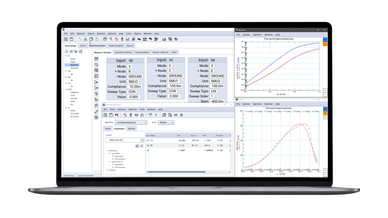
Automate semiconductor device characterization, parameter extraction, and model validation to create accurate, reliable models faster.
Device Modeling Automation
Automate device characterization and compact model generation for semiconductors.
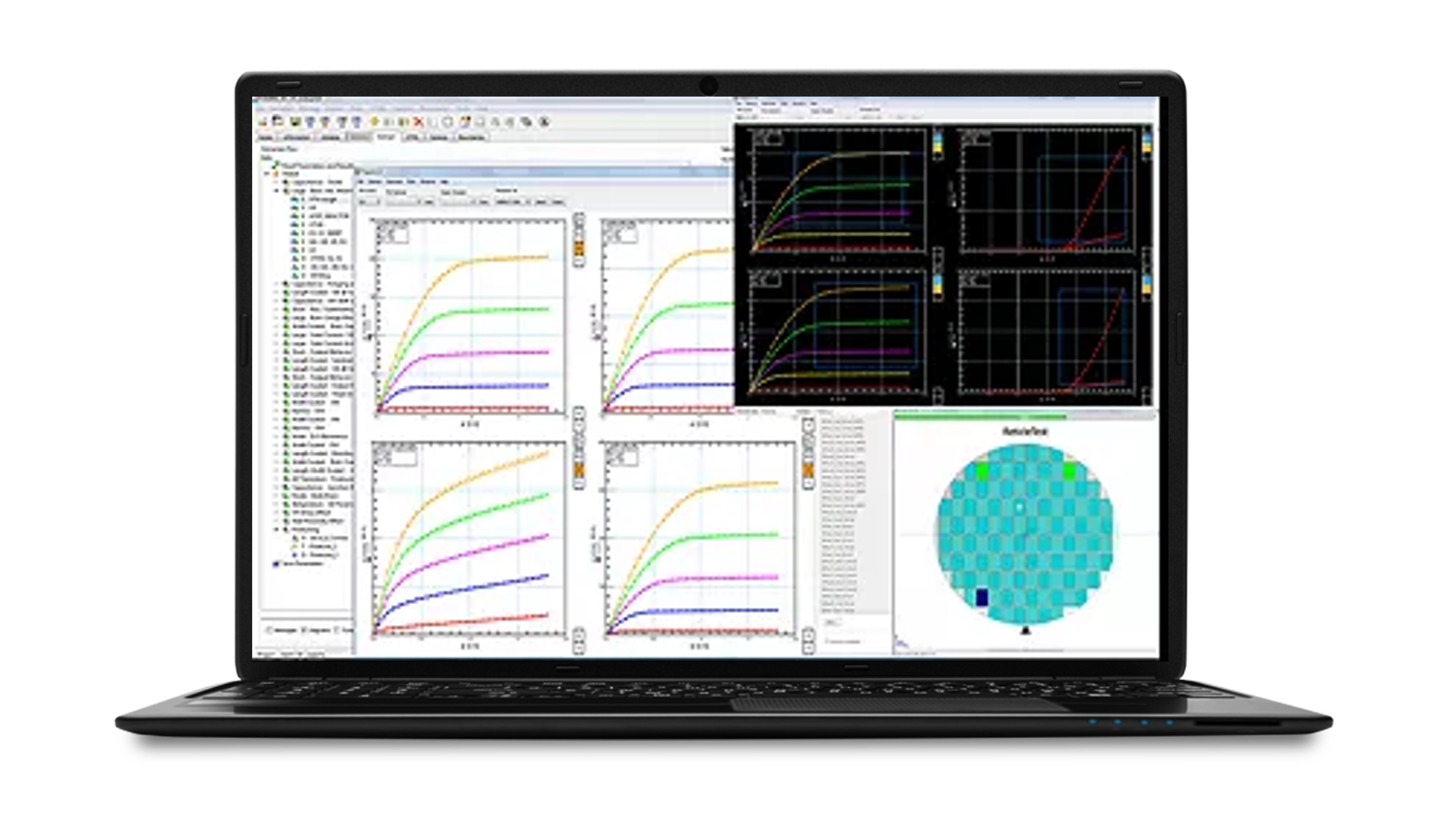
Silicon Device Modeling
Extract, optimize, and validate SPICE models for advanced silicon semiconductor devices.
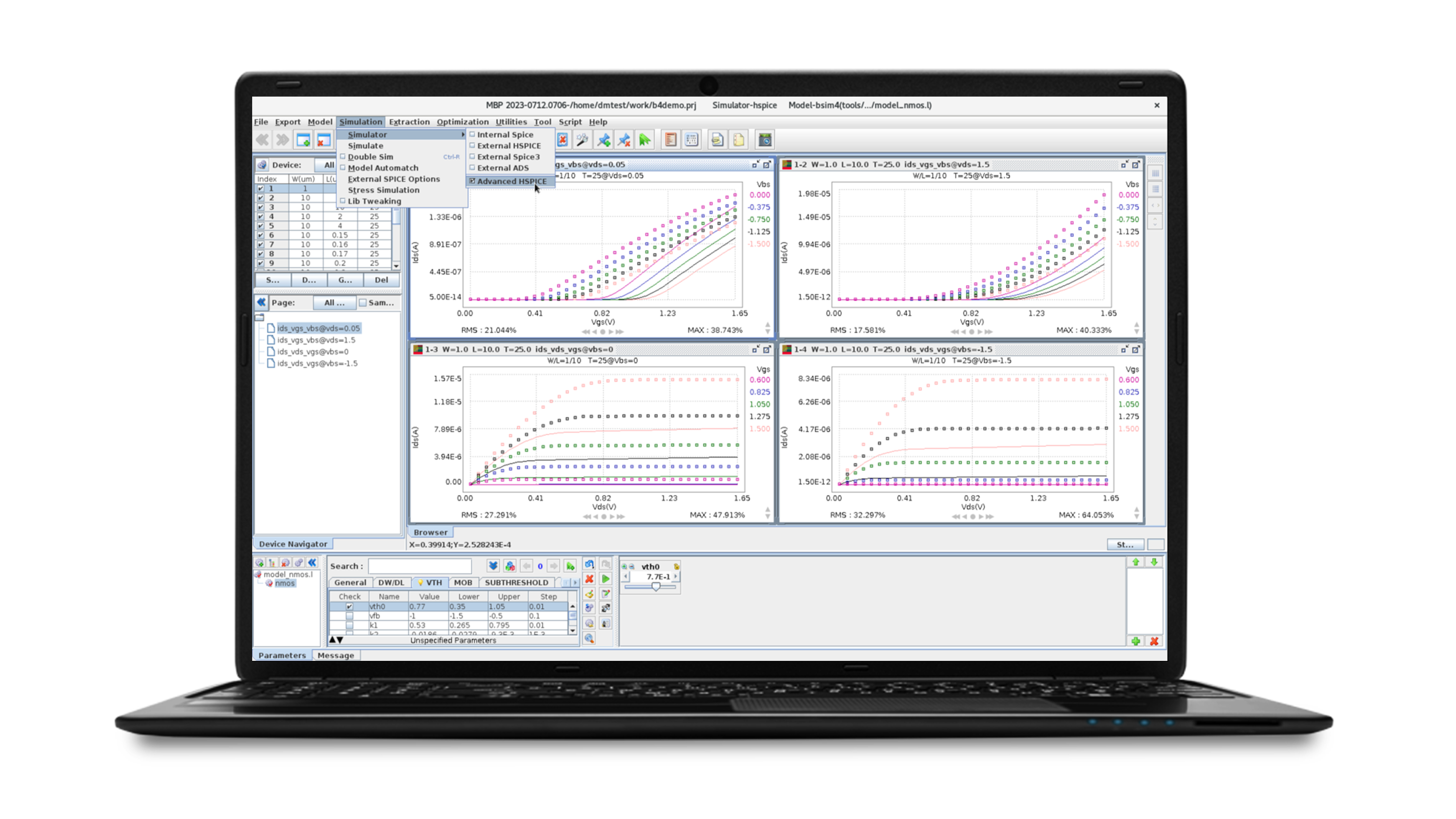
SPICE Model QA
Validate semiconductor SPICE models to ensure accuracy and consistency.
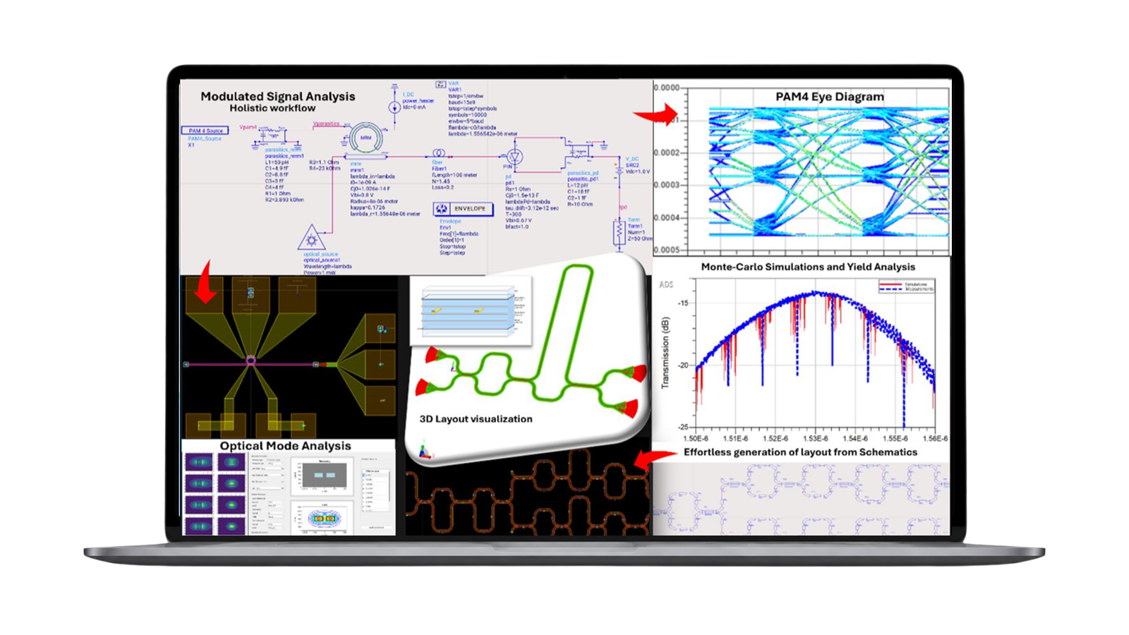
Photodetector Model Optimization
Optimize silicon photonics PIN photodetector models against measured data for accurate foundry process simulation.
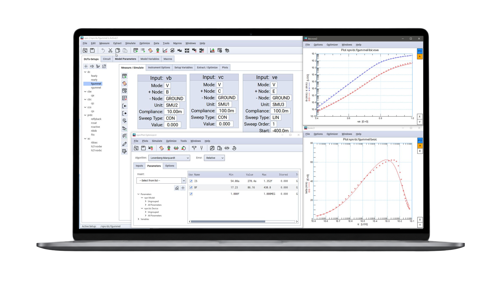
Device Model Parameter Extraction
Automate device model parameter extraction and re-centering with machine learning for faster, repeatable model development.
Centralize, track, and collaborate on semiconductor IP and design data to improve efficiency and ensure design integrity.
Design Data Management
Control and trace semiconductor design data with centralized version management.
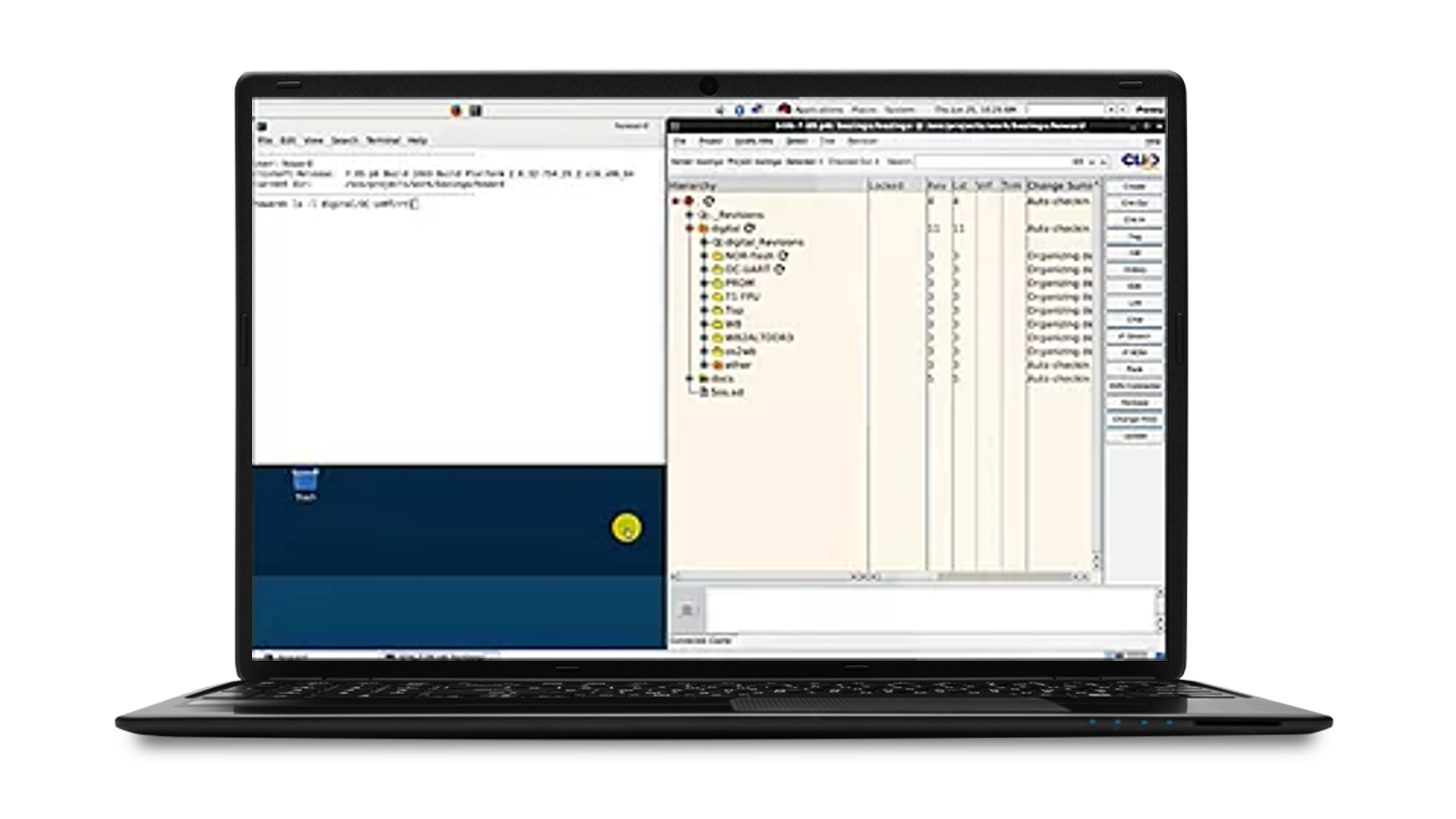
IP Management
Manage semiconductor IP lifecycles with secure storage and controlled access.

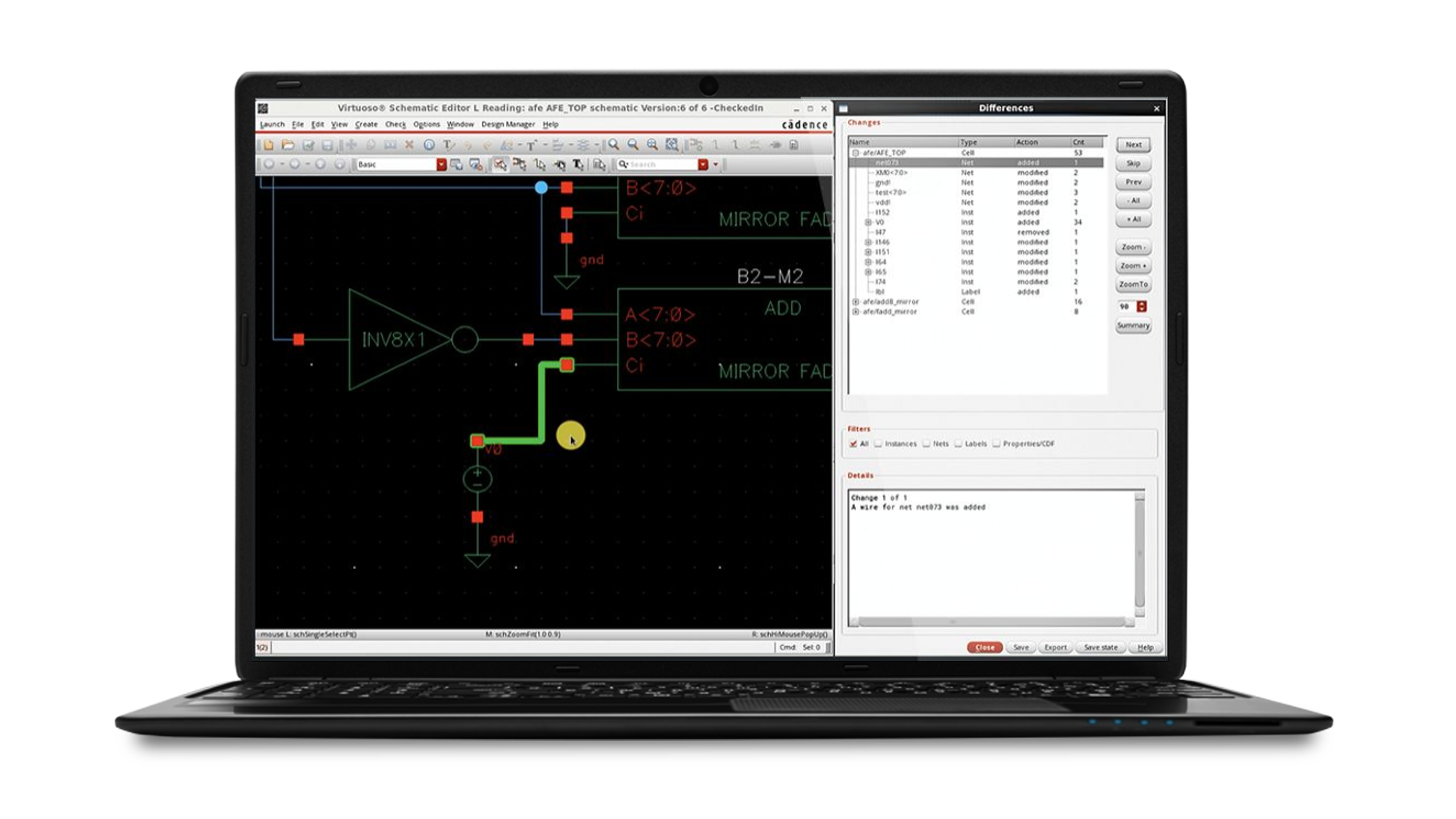
Visual Design Management
Centralize and track semiconductor design data for improved team collaboration.
Perform high-throughput wafer testing with motion control, photonics, and parametric measurements.
Silicon Photonics Wafer Test
Characterize photonic semiconductor devices at the wafer level with integrated optical/electrical test.

Fundamental Parametric Test
Measure essential semiconductor parameters with accurate, configurable test solutions.

On-Wafer RF and Sub-THz Characterization
Characterize advanced semiconductor devices at mmWave and sub-THz frequencies. Perform accurate on-wafer S-parameter and device measurements to validate next-generation RF, 5G/6G, automotive radar, and high-frequency technologies.
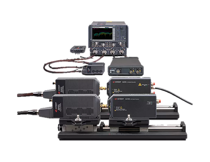
Silicon Photonics Electro-Optical Characterization
Accelerate silicon photonics development with accurate electro-optical characterization. Measure optical and electrical performance, including electro-optical S-parameters, to validate high-speed photonic devices and components.
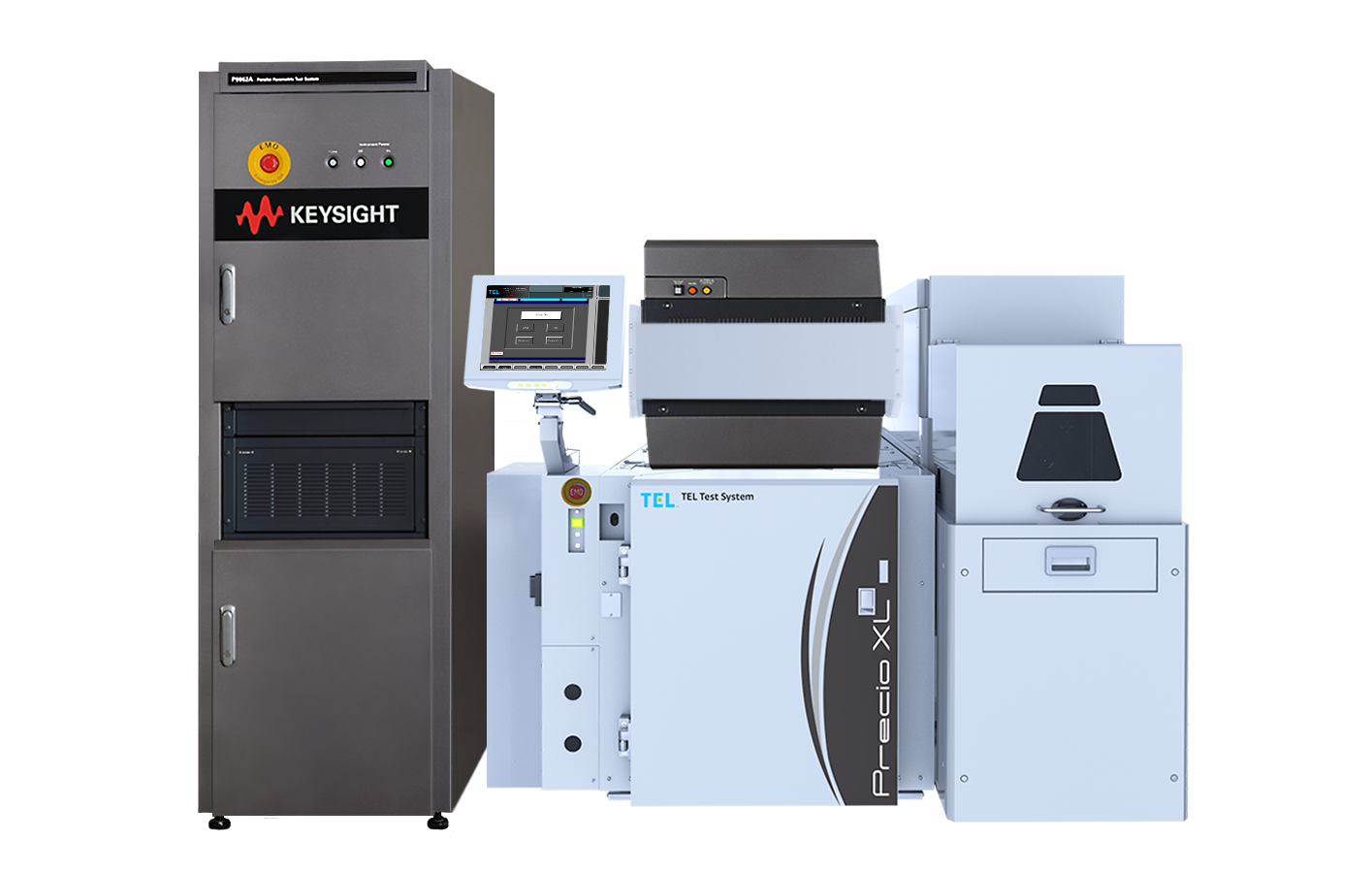
Parallel Parametric Test
Boost semiconductor testing throughput with parallel parametric measurements.
Motion Control
Enable precision motion control for wafer probing and semiconductor device test alignment.

Ensure accuracy, reliability, and high-speed operation for every design, from core measurements to system-level functionality.
Double-Pulse Test
Characterize dynamic power semiconductor devices with double-pulse testing.

Parametric Test
Deliver precision to meet parametric test / reliability and characterization tests for semiconductors.
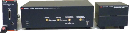
Low-Frequency Noise Analysis
Analyze low-frequency noise and assess semiconductor reliability with software that integrates with PathWave WaferPro.
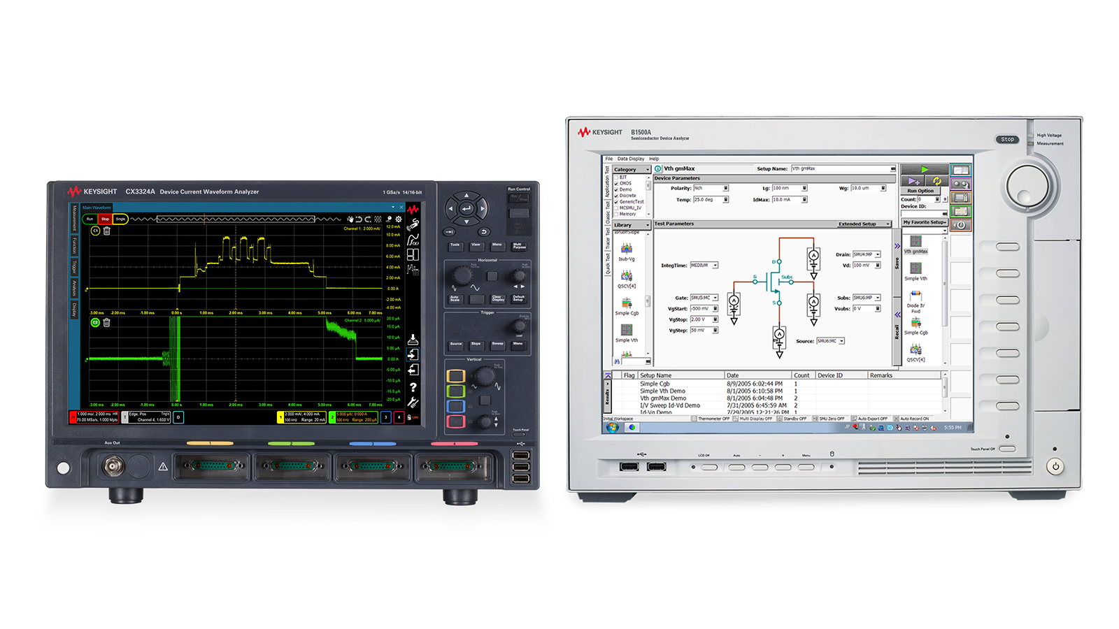
Non-Volatile Memory Device Characterization
Characterize emerging non-volatile memory devices with precise current-voltage and transient measurements.
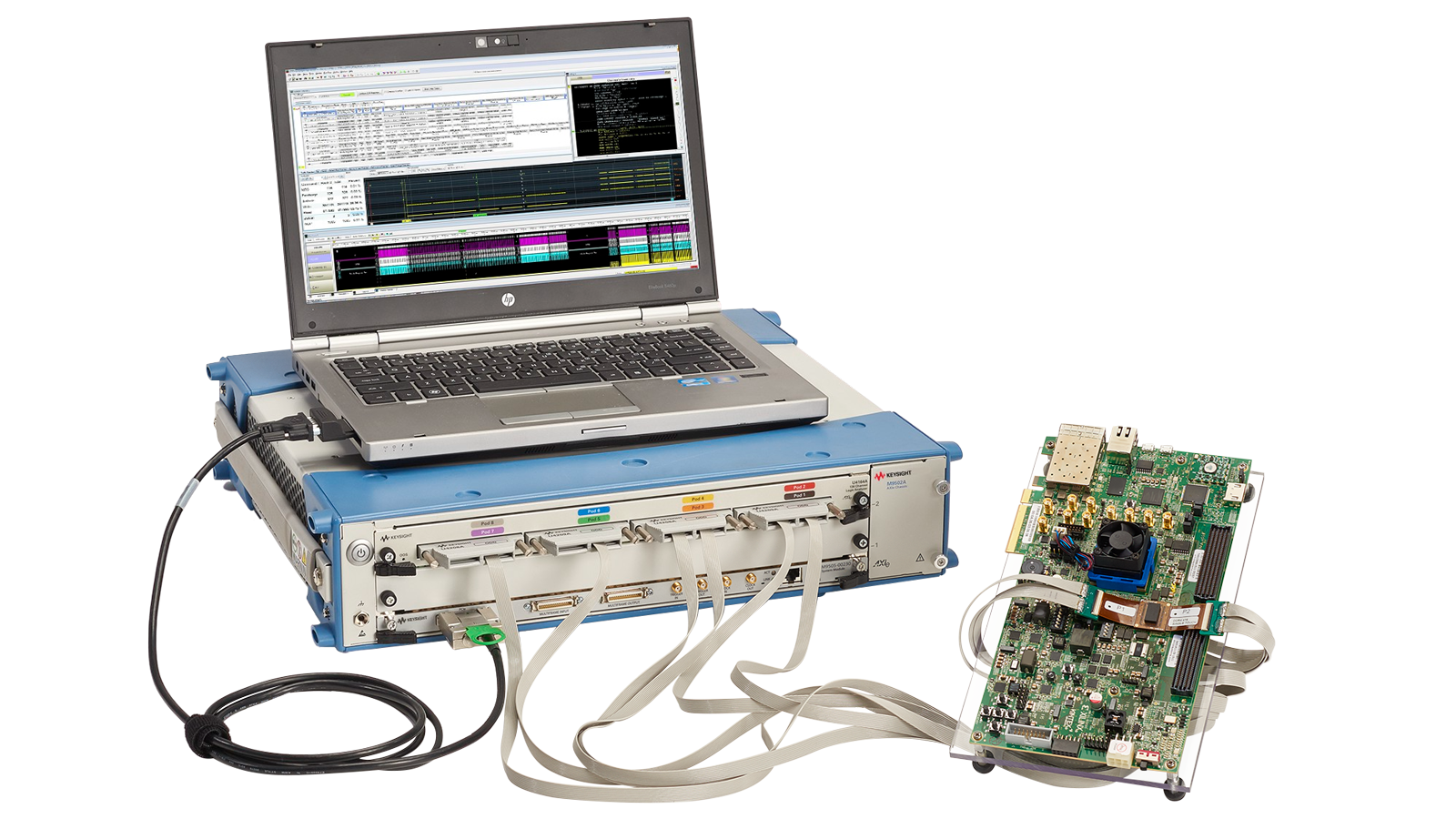
Memory Analysis
Analyze semiconductor DDR5 memory performance and timing with logic analysis.
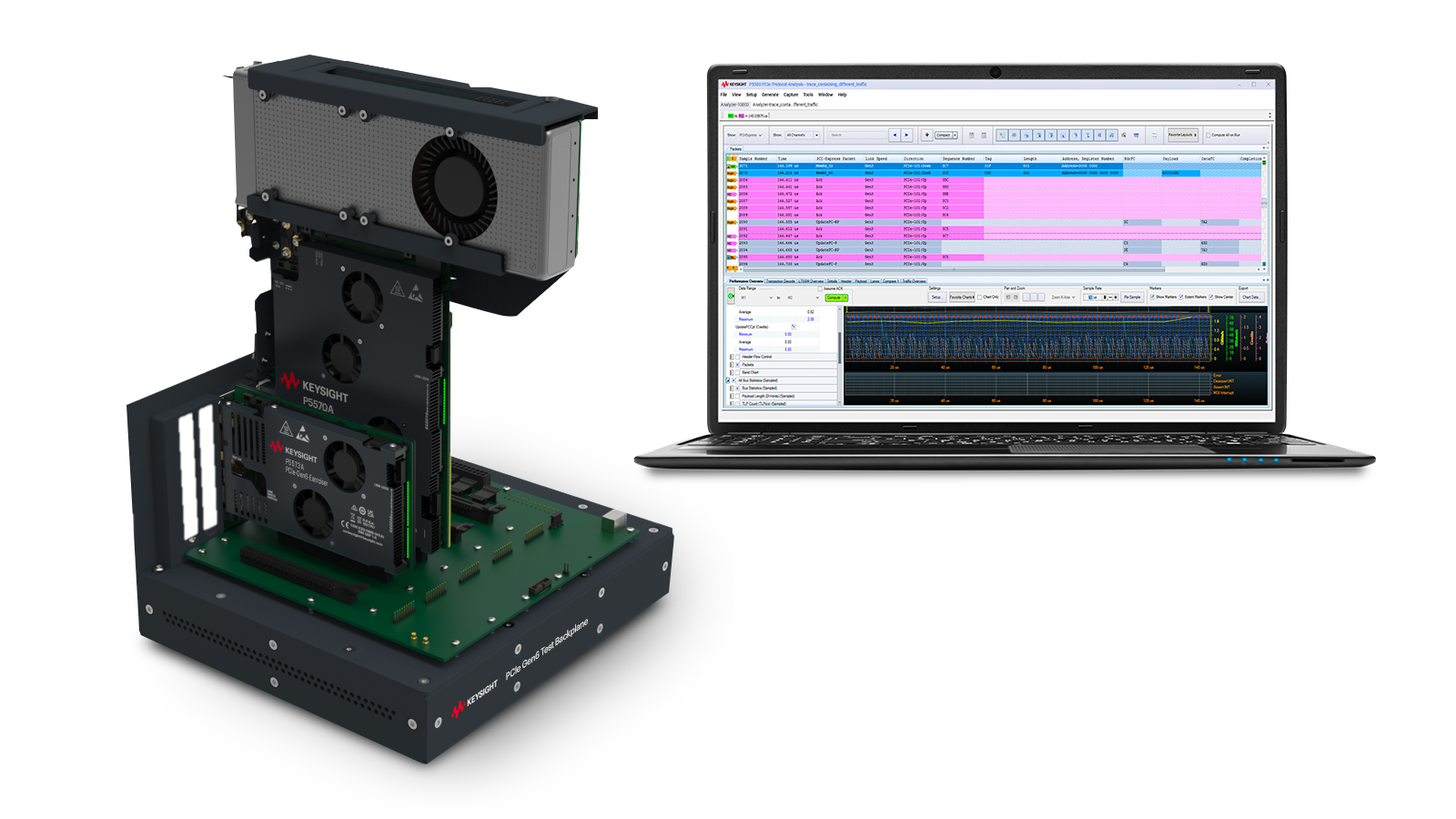
PCI Express® and CXL Validation
Validate PCIe and CXL semiconductor designs from physical layer to protocol.
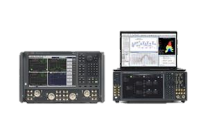
Accelerate RF and mmWave IC validation from wafer to production.

High-Speed SerDes / PAM4 Receiver Test
Validate high-speed SerDes receivers for next-generation data rates.

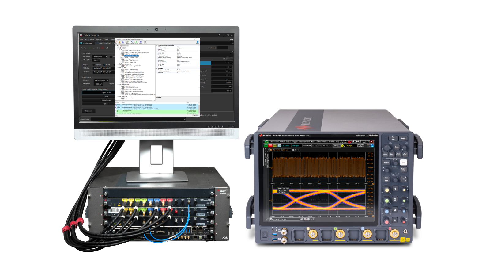
MIPI® C-PHY℠ and D-PHY℠ Validation
Validate MIPI interfaces for high-speed mobile, automotive, and embedded applications.
Low-Power IC Characterization
Accurately characterize low-power semiconductor devices and ICs.
USB4 / High-Speed Interface Validation
Validate USB4 and high-speed interface designs from transmitter to receiver.

Discover Semiconductor Teaching Lab Solution


Learn how Keysight's Semiconductor Teaching Lab helps educators quickly prepare graduates for the workforce in the semiconductor sector


Parametric Test and On-Wafer Measurement
Find out about the Keysight’s UU102LAB solution enables universities to develop industry ready graduates for the semiconductor workforce


Learn how Keysight’s UU103LAB solution enables universities to develop industry-ready graduates in photonic IC measurement and testing


Teach Tomorrow’s Chip Innovators Today
Comprehensive Semiconductor Teaching Lab Solutions equip students to innovate faster by immersing them in real‑world design, wafer‑level testing, and photonic integration.
Explore Semiconductor Use Cases
Discover Semiconductor Resources

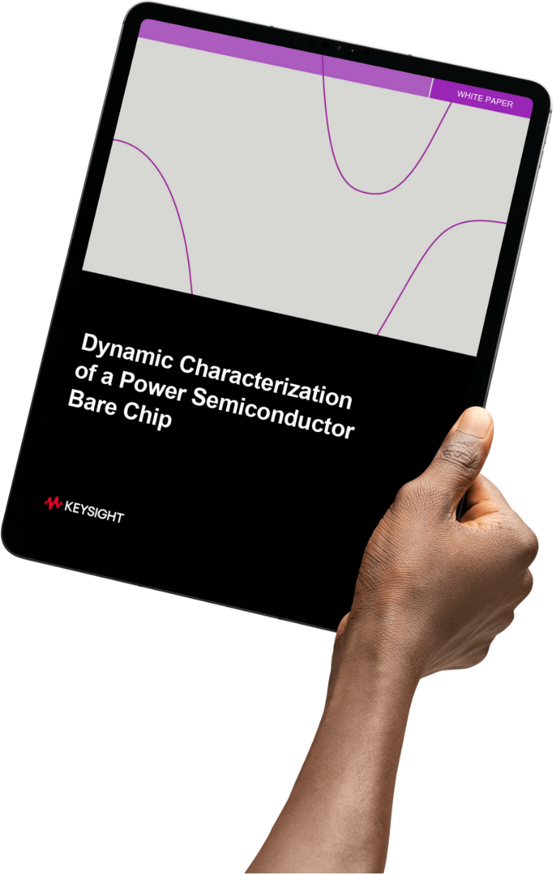
White Paper
Semiconductor Chip Characterization
Explore solutions for characterizing power semiconductor bare chips before packaging.
Learning Hub
Integrate multi-technology RF assemblies, perform semiconductor parametric testing, and explore wide-bandgap high-power semiconductor measurement techniques. Learn how.
eBook
Learn how to model GaN semiconductor devices.
Brochures
Set up a semiconductor/IC teaching lab with suggestions on everything from simulation to validation and experiments.
eBook
Semiconductor IP enables a modular approach to system on a chip (SoC) design. Explore 6 steps to effective IP management.
Let's Solve What's Next.
Book a meeting or demo with one of our experts