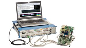
Performing DDR4 functional validation and protocol debug
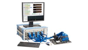
Implementing a double data rate 4 (DDR4) memory system requires engineers to perform thorough read / write functional tests. They require a solution that can quickly step through, isolate, and uncover issues, such as memory write-back, initialization, system crashes, and system abnormalities. To perform a complete protocol validation and performance improvement of DDR4 systems, test engineers need a logic analyzer that can stream bus signals and record them at specific data rates.
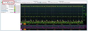
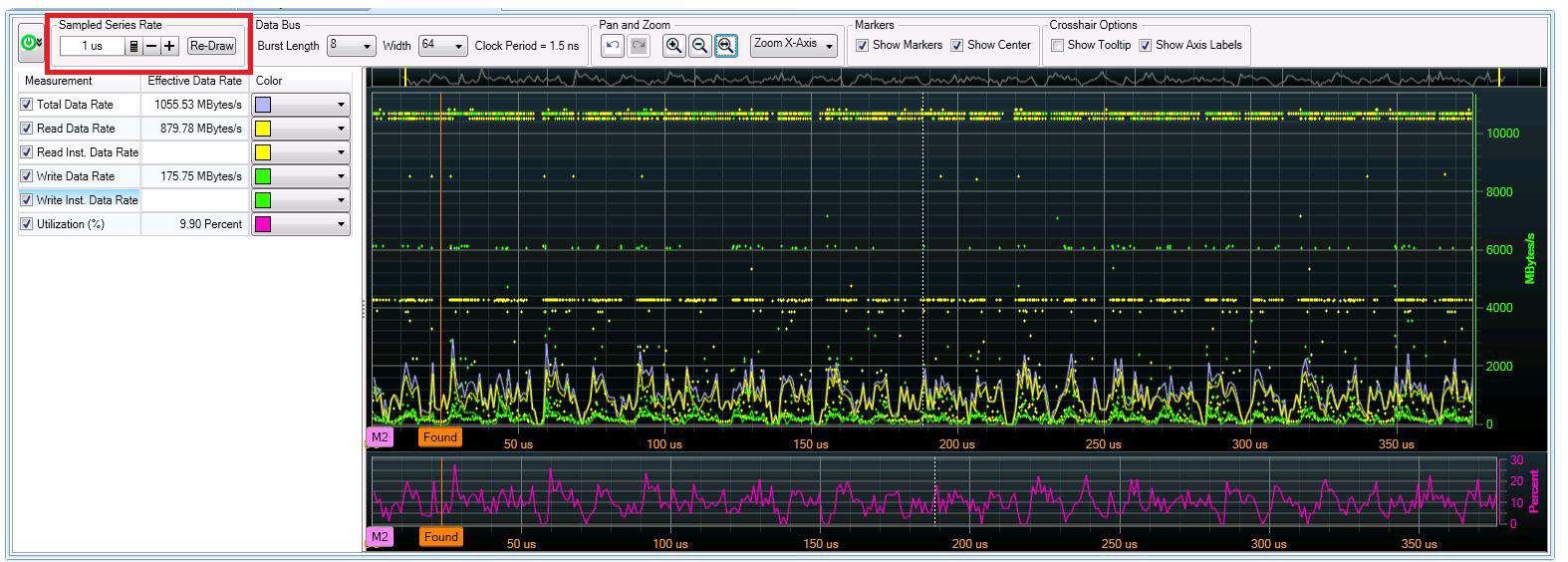
Special DDR4 dual in-line memory module (DIMM) or ball grid array (BGA) hardware interposers are required to capture the complete bus trace signals reliably. Memory analysis software is critical to analyze the performance and functional protocol compliance, including post-process compliance violations across speed changes. Engineers should also monitor memory performance with qualitative insights for hundreds of signals and bus-level signal integrity.
DDR4 test and debug solution
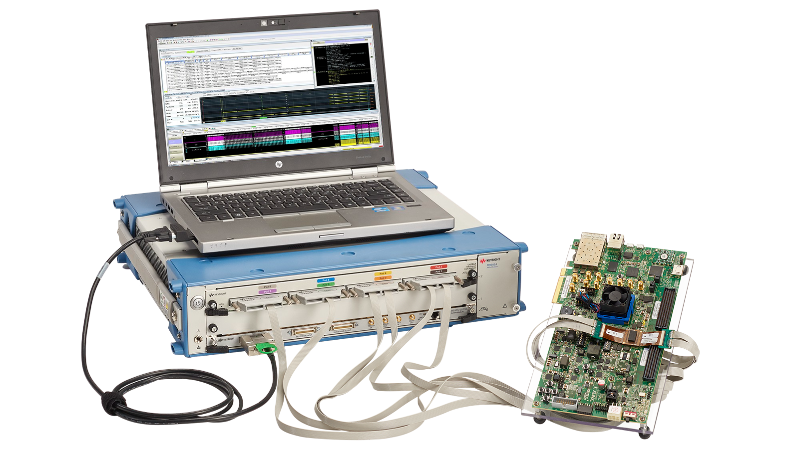
Testing and debugging DDR4 memory systems require engineers to perform functional / protocol validation, debugging, analysis, and bus-level signal integrity testing. The Keysight solution for DDR4 is a complete test, debug, and analysis solution. It consists of an interposer, a high-performance logic analyzer, and memory analysis software. Different interposers enable connectivity to different memory packages, including DIMM, SODIMM, or BGA. The high-performance logic analyzer should stream all the bus signals and record them at data rates up to 5,000 Mb/s for address and command and up to 4,000 Mb/s for data. The memory analysis software executes performance and functional protocol analysis. The Keysight DDR4 solution also provides a visual, qualitative DDR eye-scan tool that enables you to scan hundreds of bus-level signals simultaneously to assess the system’s signal integrity quickly.
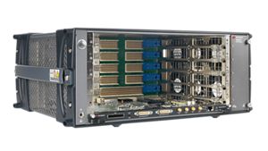
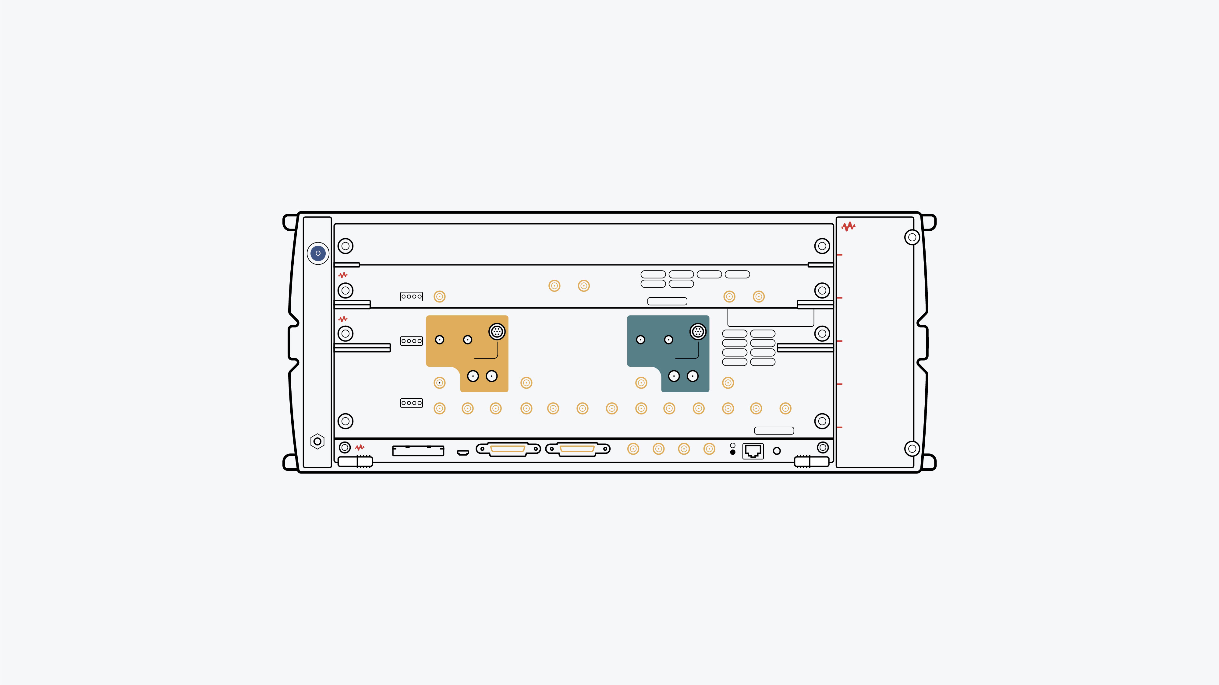
M9505A 5-slot AXIe chassis with embedded system module and Gen 2, x8 link to external controller.
Slots
5 slots
Form Factor
AXIe
Height
4U
Slots
5 slots
Bandwidth
4 GB/s
Connectivity
LAN
PCIe
How to Test and Debug DDR4 Systems
B4661A Memory Analysis Software for Logic Analyzers
Achieve greater insight faster using the B4661A memory analysis software and your Keysight logic analyzer system for debug and validation of DDR3, DDR4, DDR5, LPDDR2, LPDDR3, LPDDR4, or LPDDR5 systems.
U4164A Logic Analyzer Module with State Mode up to 4Gb/s
The U4164A logic analyzer provides industry’s highest data rate state mode (up to 4 Gb/s), highest deep trace timing mode (up to 10 GHz), and deepest memory (up to 400 Mb), enabling validation and debug of DDR4 or LPDDR4 at data rates over 3.5 Gb/s.
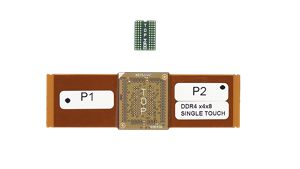
W4643A DDR4 x4/x8 BGA Interposer for Logic Analyzer, Connects to 61-pin ZIF
The W4643A DDR4 x4/x8 - 2 wing BGA interposer for 78-ball DDR4 DRAM. It is designed for data rates up to and including 3.3 Gb/s. It captures all ADD/CMD/DQ/DQS.