Semiconductor Modeling and Characterization
Turnkey solutions for device modeling and characterizing CMOS, RF, and III-V devices.

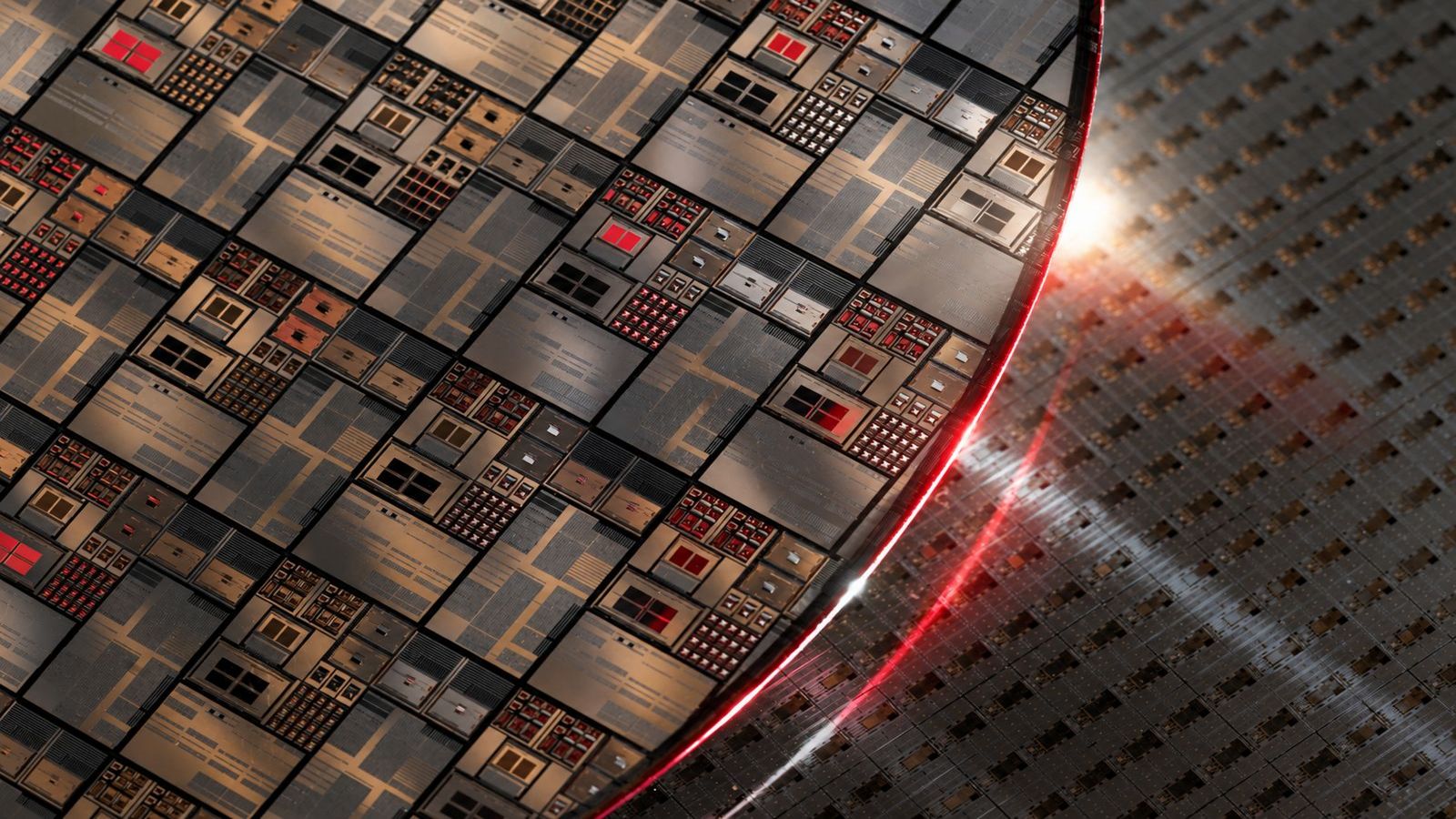


Simplify modeling for silicon CMOS, Bipolar, GaAs, GaN, and other advanced IC technologies with integrated measurement, simulation, optimization, and statistical analysis in one solution.

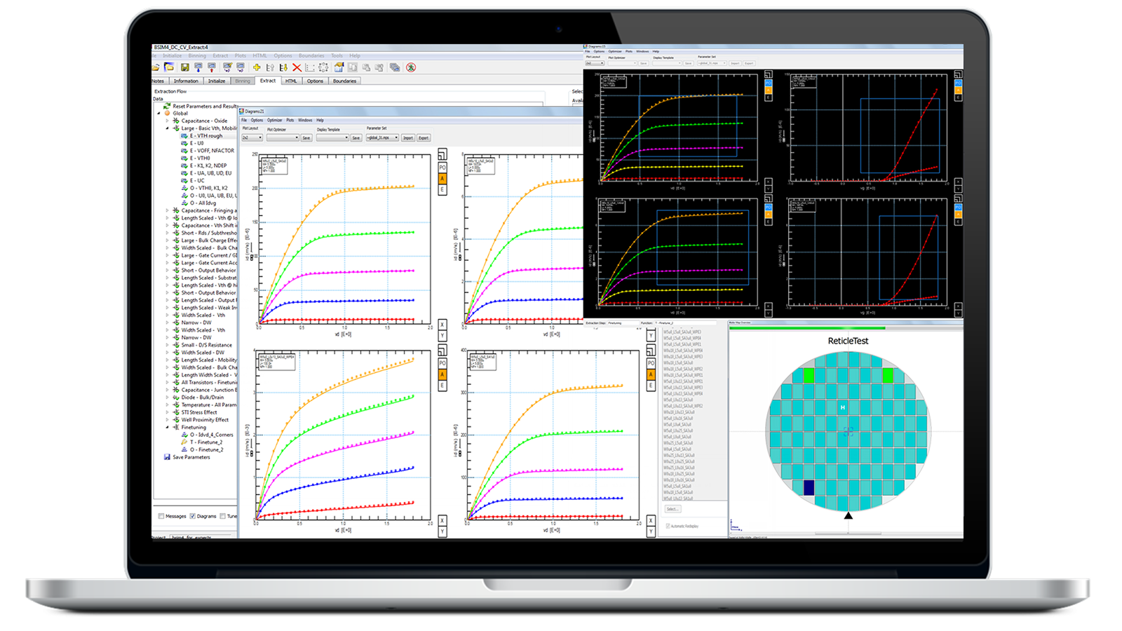
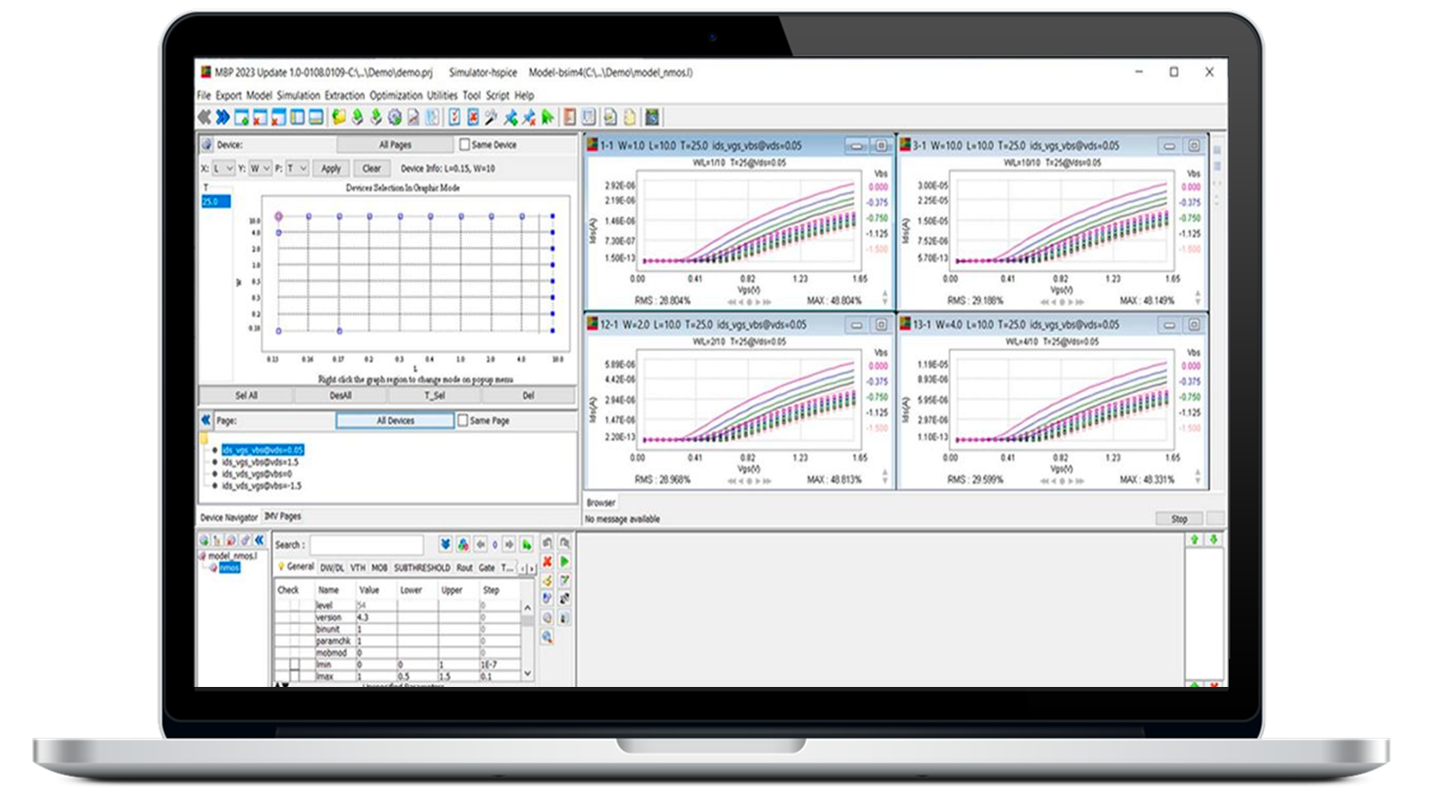
Complete silicon turnkey device modeling software that integrates SPICE modeling and simulation, model parameter extraction, and model library generation.

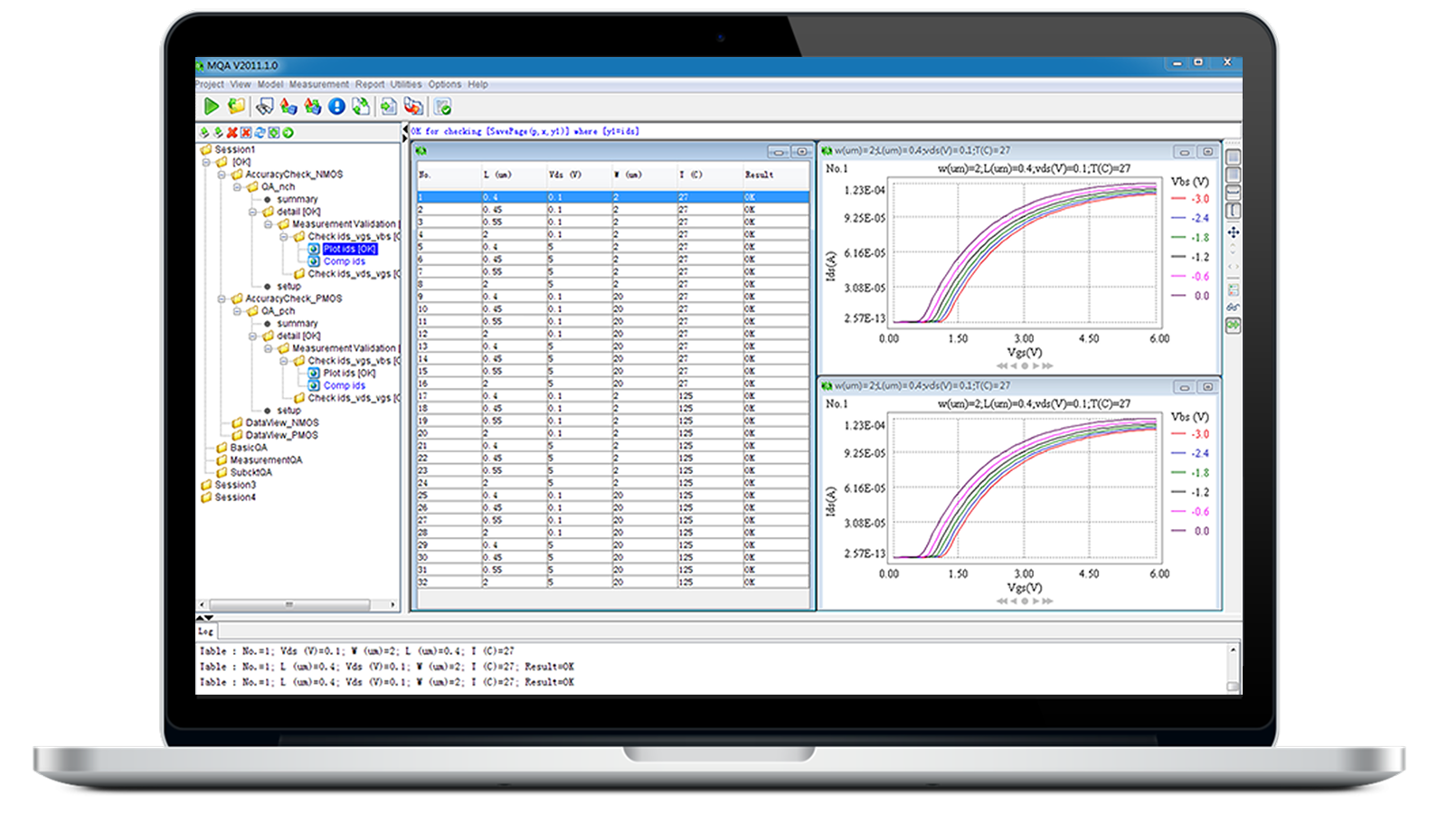
Model QA (MQA) is a collection of comprehensive SPICE model validation procedures, interfaces, and utilities that provide the ability to thoroughly check SPICE model quality and automate QA and reporting procedures.

Perform automated wafer-level measurements of semiconductor devices such as transistors and circuit components. The software provides turnkey drivers and test routines for various instruments and wafer probers including the Keysight A-LFNA.


Develop Process design kit, assess manufacturing statistical process control and reliability, and verify the IC noise specifications.
Learn from Industry Experts
Foundry leaders will need to focus strategically on modernizing workflows to boost productivity and unlock areas of opportunity. Keysight works in close collaboration with foundries to deliver highquality models and PDKs tailored for Si, SiGe, GaAs, InP, and GaN processes. Our software and services form a total solution covering test structure design, device characterization and modeling, PDK creation, validation, and process and data management.


Blogs
Bootcamps
More Resources
eBooks
The Essential Guide to GaN Semiconductor Device Modeling

White Papers
Accelerating Semiconductor Innovation through Machine Learning-Driven Modeling
WEBINARS
Simplifying and Automating Compact Model Process with Machine Learning
WEBINARS
RTN Measurement and Stress-testing using A-LFNA/WaferPro
Semiconductor Modeling and Characterization FAQs
Device modeling creates mathematical representations of semiconductor devices that predict electrical behavior under varying operating conditions, enabling accurate simulation and design optimization before hardware fabrication.
The solutions support a wide range of technologies, including CMOS, bipolar, GaAs, GaN, RF, compound semiconductor, and wide-bandgap devices used in advanced electronic and photonic applications.
Device characterization captures measured electrical data across operating conditions, providing the foundation for parameter extraction and ensuring models closely represent real device behavior.
Yes. Automated extraction, validation, and model quality assurance workflows help reduce modeling effort, improve consistency, and speed the delivery of high-quality PDKs.
Model validation verifies that extracted models remain accurate across bias, geometry, temperature, and frequency ranges, ensuring reliable circuit simulation and design results.