


- Overview
- All Models
- Support
Scalable platforms for wafer-level and packaged semiconductor validation
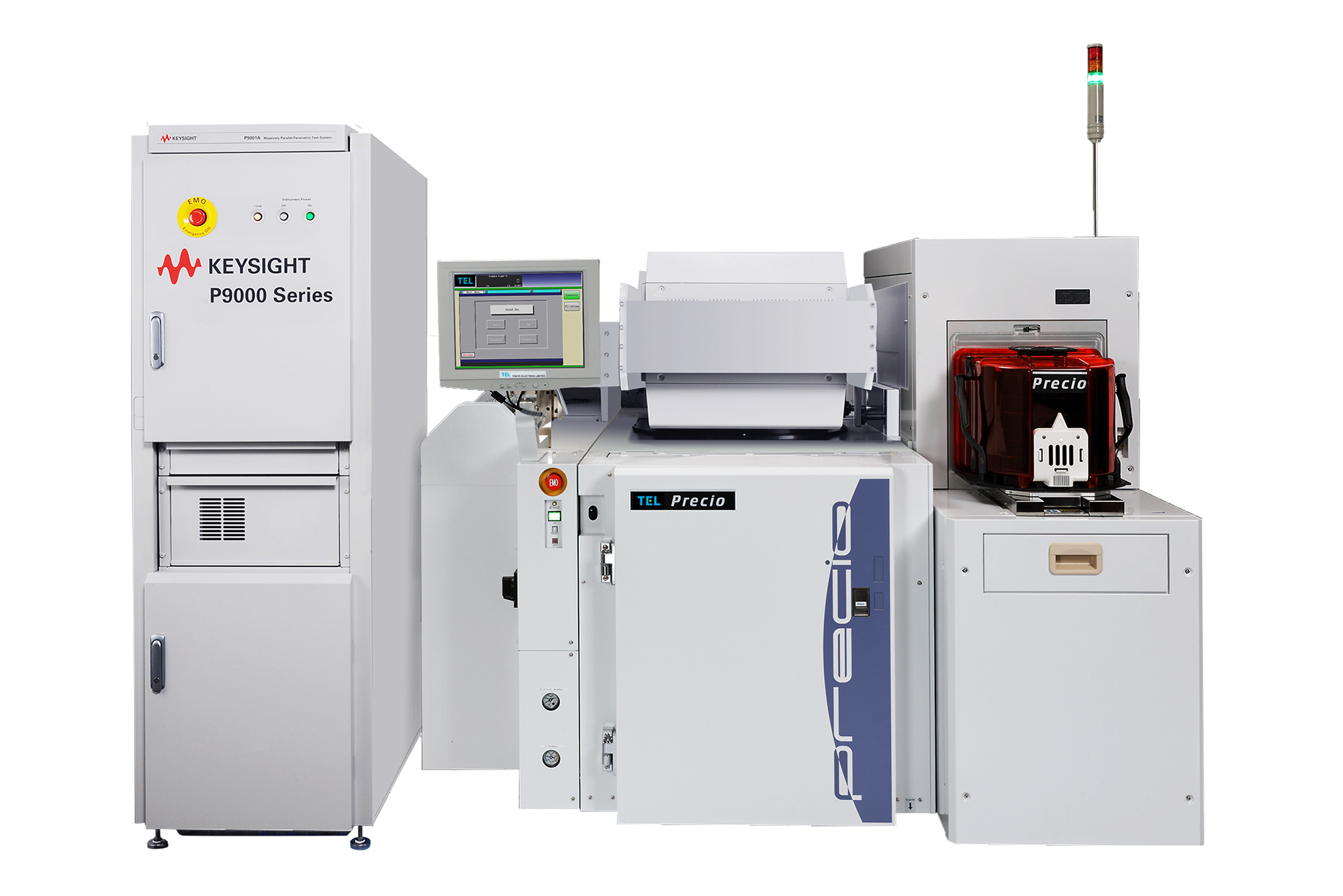
Keysight parametric test solutions combine high-performance measurement instruments with flexible automation to accelerate semiconductor device evaluation from early development to high-volume production. Offering precise current-voltage (IV), capacitance-voltage (CV), and reliability testing, these scalable systems help optimize device performance, monitor process variability, and ensure long-term reliability. Designed for seamless integration with wafer probers and production environments, Keysight parametric solutions deliver the accuracy, speed, and efficiency needed for today’s advanced semiconductor technologies. Request a quote for one of our popular configurations today. Need help selecting? Check out the resources below.
High-throughput automation
Increase test efficiency with multi-site capabilities and fast, programmable switching, ideal for use in volume wafer probing or high-mix packaged device environments.
Flexible test integration
Seamlessly combine precision SMUs, capacitance measurement units, pulse modules, and reliability tools within one scalable system to suit a wide range of test scenarios.
Process and reliability focus
Perform comprehensive parametric, pulsed IV, and long-duration stress measurements to support device qualification and monitor reliability across different operating regimes.
Customizable software
Leverage modular software platforms to tailor test sequences and automation scripts for production, modeling, or exploratory device research.

-
Minimum current measurement resolution
0.1 fA to 1 pA
-
Minimum voltage measurement resolution
2 µV
-
Maximum number of measurement pins
2 to 100
-
Additional features
CV measurement, SPGU output, One-pass optical & electrical test, High voltage CV measurement
Most popular configurations
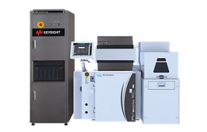
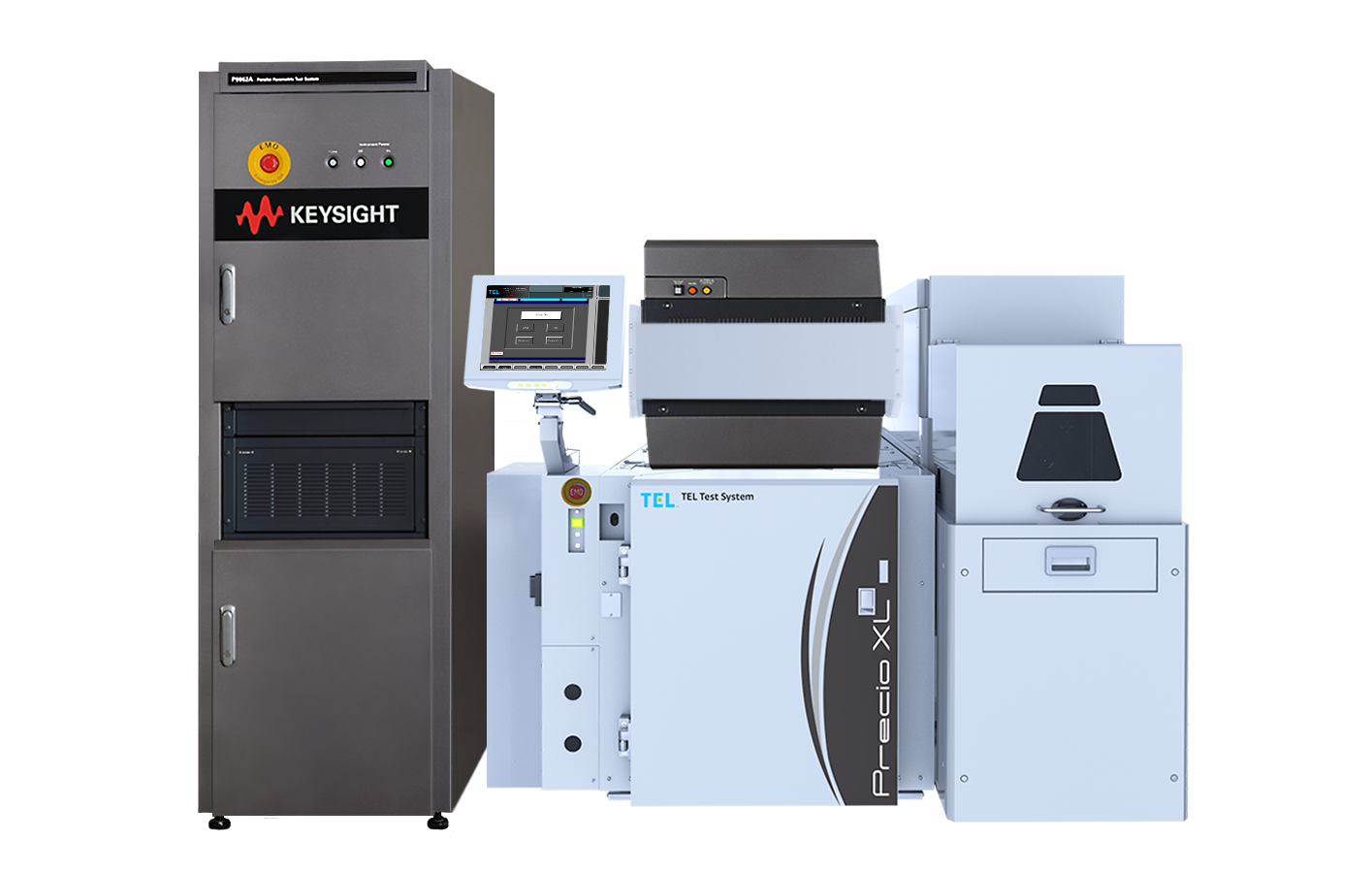
Parallel Parametric Test System
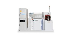

4080 Series Parametric Test Systems
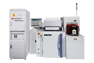
Massively Parallel Parametric Test System
- The Parametric Measurement Handbook
- Impedance Measurement Handbook
Services and support
Innovate at speed with curated support plans and prioritized response and turn-around times.
Get predictable, lease-based subscriptions and full lifecycle management solutions—so you reach your business goals faster.
Experience elevated service as a KeysightCare subscriber to get committed technical response and more.
Ensure your test system performs to specification and meets local and global standards.
Make measurements quickly with in-house, instructor-led training, and eLearning.
Download Keysight software or update your software to the newest version.
Frequently asked questions
Parametric test solutions are comprehensive systems used to electrically characterize semiconductor devices and monitor process parameters across fabrication, modeling, and reliability workflows. Unlike functional testers that verify digital logic or analog behavior, parametric testers measure fundamental electrical properties such as resistance, capacitance, threshold voltage, leakage current, and dielectric strength. These systems integrate high-precision instruments, including SMUs, CV meters, and switching matrices, with automation software and wafer probe interfaces. Parametric testers are designed for high accuracy and repeatability, often supporting parallel test sites and fully automated probe station control. This enables rapid, non-destructive testing of key device characteristics during process development, lot qualification, and production monitoring. Their scalability and automation readiness set them apart from benchtop analyzers or standalone instruments.
In semiconductor fabs, parametric test systems are deployed in-line and end-of-line to monitor critical parameters that affect device performance and yield. During wafer fabrication, process control monitors (PCMs) or test structures are placed alongside functional devices. Parametric testers probe these structures to evaluate gate oxide integrity, junction leakage, line resistance, via reliability, and transistor characteristics. The collected data helps engineers detect lithography, etch, implant, or annealing issues before they impact production wafers. Results are fed into statistical process control (SPC) systems to track trends, identify excursions, and implement corrective actions. In high-volume environments, parametric testers must provide fast settling times, accurate low-current measurements, and multi-site capability to ensure high test throughput without compromising measurement fidelity.
Parametric test solutions support a broad range of test types, covering both device-level and process-level evaluation. These include:
- DC IV tests: Gate, drain, and bulk current measurements; threshold voltage and leakage assessments; on/off ratios and resistivity.
- CV measurements: Capacitance-voltage profiling to extract doping profiles, oxide thickness, and interface trap density.
- Pulsed measurements: Used to avoid thermal effects in power devices or extract dynamic parameters.
- Stress testing and reliability characterization: Time-dependent dielectric breakdown (TDDB), bias temperature instability (BTI), hot carrier injection (HCI), and electromigration tests.
- Wafer-level testing: Non-packaged devices are probed at the die level across 6", 8", or 12" wafers using automated probers.
These solutions are commonly used with CMOS, FinFET, RF devices, power semiconductors, and new material devices such as GaN, SiC, or 2D transistors. Engineers can configure the test plan to match device complexity, technology node, and reliability qualification standards.
Test automation is a cornerstone of modern parametric test systems, especially in wafer-level and production environments where throughput and consistency are critical. Automation encompasses hardware-level control (e.g., wafer loader, prober, thermal chuck), test execution (e.g., multi-site sequencing, fast relay switching), and data analysis/reporting. Software platforms such as Keysight’s WaferPro Express or other customizable automation suites enable the creation of test plans with graphical workflows, conditional branching, and looping. Parallel testing, where multiple dies are tested simultaneously, significantly reduces test time per wafer. Additionally, integration with yield management systems and database tools allows for real-time data logging, statistical process control, and correlation with downstream electrical test or failure analysis data. All of these capabilities reduce human error, speed up time-to-yield, and enable scalable, repeatable test strategies across global fabs or labs.
Choosing a parametric test system for advanced technologies involves careful consideration of performance, scalability, and integration. Key factors include:
- Measurement capability: Ensure the system supports femtoamp-level current sensitivity, high-speed voltage sweeps, and accurate capacitance measurements suitable for scaled geometries and advanced materials.
- Channel density and flexibility: High-pin-count devices and test structures require systems with a large number of channels and flexible switching configurations.
- Reliability stress capability: Evaluate whether the system supports long-duration biasing, temperature control, and automated logging for TDDB, BTI, or NBTI studies.
- Wafer prober integration: Full automation requires compatibility with popular prober brands and support for wafer mapping, alignment, and temperature chuck control.
- Software ecosystem: Look for solutions with intuitive test scripting, real-time data visualization, pass/fail reporting, and SPC integration. Compatibility with external analysis tools (e.g., Python, JMP, MATLAB) enhances flexibility.
- Modular scalability: Ensure the system can be expanded as device complexity grows—such as support for more sites, additional instruments, or new test routines—without major reconfiguration.