Choose a country or area to see content specific to your location
What are you looking for?
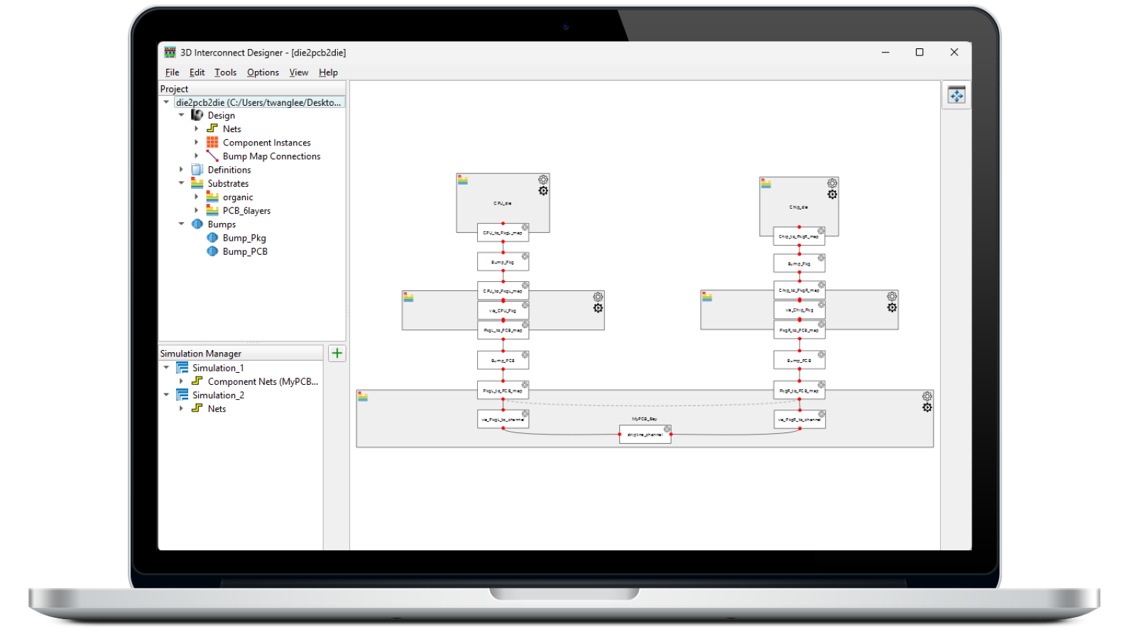
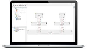
Design, model, and validate complex 3D interconnect architectures with a powerful standalone design environment.
Automate transmitter and receiver validation across next-generation I/O, memory, and fabric interfaces.
Strengthen 1.6T network reliability for AI-scale workloads from transceivers to interconnects.

Pair Keysight VSA software with the new XA5 signal analyzer for advanced visualization, demodulation, and analysis — start your 30-day trial today.
With extra memory and storage, these enhanced NPBs run Keysight's AI security and performance monitoring software and AI stack.
Explore end-to-end workflows spanning IC design, validation, wafer test, and photonics.

Save up to 50% on our latest instruments with eligible Keysight or competitor trade-ins.
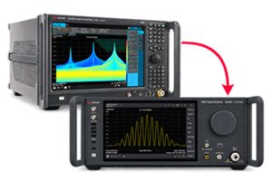
Achieve 200+ Gbaud multi-level modulated signals with high-speed AWGs for digital and optical standards.
Maximize accuracy and performance with precision accessories engineered for Keysight instruments.
Save up to 50% on our latest instruments with eligible Keysight or competitor trade-ins.
Four channels per 1U of rack space, up to 1 GHz bandwidth, and multi-oscilloscope synchronization.
Purpose-built solutions engineered for the design and test challenges unique to your industry.
Use Cases mapped to every stage of your product lifecycle, from design through operations.
Success Stories
Authoritative application notes, data sheets, reference designs, and test procedures to accelerate design and validation decisions.
Hands‑on bootcamps that teach system design, test methods, and production workflows engineers can apply immediately.
Learning Hub
Explore methodologies, test strategies, and technical resources for designing, validating, and scaling AI systems and networks.
Quick access to support related self-help tasks.
Additional content to support your product needs.
Explore services to accelerate every step of your innovation journey.
Accelerate RF, High-Speed Digital, Power, Photonic, and Quantum Design with Industry-Leading Simulation.
Premier RF and high-speed digital EDA platform.
Keysight ADS is the premier electronic design automation (EDA) platform for the design of high-frequency RFICs, RF transceiver modules and RF PCBs. Its highly accurate multi-domain RF circuit-EM-electrothermal and system simulators, complemented with industry standards compliant test bench libraries, makes ADS sought after also for High-Speed Digital, Quantum, Power Electronics and Silicon Photonics applications.
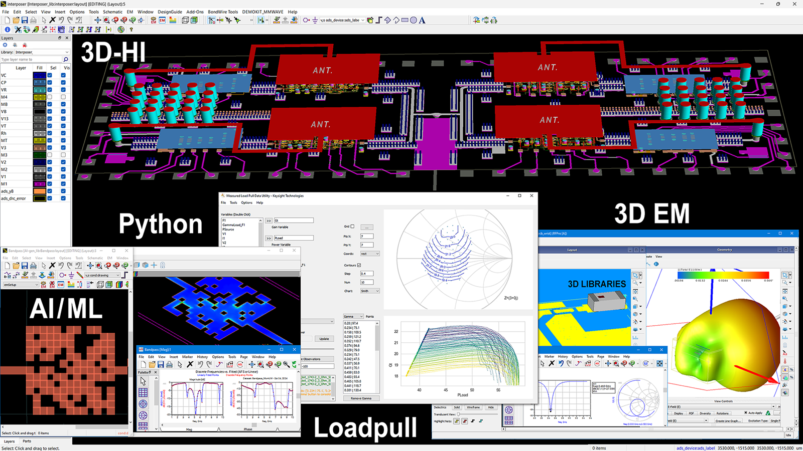
ADS is an integrated design, simulation and optimization platform with unique 3D Heterogeneous Integration (3DHI) drag-and-drop advanced packaging of RF transceiver modules and chiplets. The ADS industry standards compliant test benches covers both wireless and high-speed digital standards with Keysight instrument grade algorithms for signal generation and analysis to ensure the highest verification accuracy and eliminate wasteful hardware respins.
ADS provides an open environment with AI Model Context Protocol (MCP) interface and Python APIs to enable complex workflows to be captured and orchestrated for efficient, parallelized design exploration and optimization of even the most challenging multi-objective design.
Design chips, packages, boards, and interconnects together.
Accurately model complex electromagnetic behavior before prototyping.
Combine circuit and EM analysis for higher accuracy.
Generate models from measured and published data.
Automate design processes using Python scripting integration.
Enable interoperability across leading EDA environments.
As radio-frequency (RF) applications move into millimeter-wave (mmWave) frequencies, integration is becoming denser. This density increases the complexity of correctly assembling, simulating, and verifying multi-technology RF modules. Keysight's ADS helps reduce costly hardware failures by enabling a 3D Heterogeneous Integration (3DHI) of RFICs, MMICs, packaging, PCBs, and antennas into multi-technology modules.
Signal and power integrity are becoming more important as frequency and speed increase in printed circuit boards (PCBs). Losses associated with transmission line effects can cause failures in electronic devices. Modeling traces, vias, and modern interconnects such as Chiplets UCIe and BoW are necessary to simulate the board accurately. Improve high-speed link performance in PCB designs with standards-driven integrated circuit design and electromagnetic simulators customized for power and signal integrity analysis.
Power supplies, solar inverters, and electric vehicles are driving the need for more efficiency in power device designs. The technology that enables an increase in efficiency is wide-bandgap materials such as Silicon Carbide and Gallium Nitride. Model modern materials and switch-mode power supplies to optimize power device designs for maximum efficiency.
Keysight's Photonic Designer is a cutting-edge Electronic Photonic Design Automation (EPDA) solution engineered to meet the complex demands of photonic integrated circuit (PIC) design. By seamlessly integrating physics-based simulations with measurement-calibrated models, our software empowers engineers to design, simulate, and validate PICs with unmatched accuracy.
As the demand for more powerful quantum chips grows, innovative quantum design is key to accelerating development. Save time and cut costs with intuitive tools that bridge the quantum knowledge gap for microwave engineers. Stay ahead in the quantum race—embrace cutting-edge design to fuel breakthroughs in computing and beyond. Transform possibilities into reality with speed and precision. Unlock the future with Quantum Design!
Complex product designs need massive and time-consuming simulations. Keysight Design Cloud leverages High-Performance Computing (HPC) technologies that let you run parallel simulations in the cloud, cluster, or server to reduce simulation time and expedite time-to-market significantly.
ADS Software Bundles provide circuit and component designers with a choice of value-packed, preconfigured combinations of software modules built for specific design workflows. These combinations start with the powerful core ADS functionality for 3D physical layout and verification, data display, optimization, Python scripting automation and statistical analysis.
blogs
blogs
blogs
blogs
blogs
blogs
blogs
Technical Overviews
eBooks
eBooks
eBooks
eBooks
eBooks
Discover the latest release designed to help engineers work faster, simulate more accurately, and accelerate product development.
ADS is an electronic design automation platform used to design and simulate RF, microwave, high-speed digital, power electronics, photonic, and quantum systems before hardware development.
ADS minimizes costly design iterations by enabling accurate circuit, electromagnetic, electro-thermal, and statistical simulation before physical prototypes are built.
Yes. ADS supports 3D heterogeneous integration workflows that combine chips, packages, PCBs, interconnects, shielding, connectors, and antennas within a unified design environment.
Yes. ADS includes specialized capabilities for signal integrity, power integrity, high-speed serial links, memory interfaces, and advanced interconnect technologies.
ADS brings together circuit simulation, electromagnetic analysis, AI-assisted modeling, automation, and open-architecture interoperability in a single platform, helping engineers solve complex multi-domain design challenges faster.
Talk to our team to find the right solution for your design needs, get a personalized quote, or request a free trial.
What are you looking for?