Here's the page we think you wanted.
See search results instead:
Choose a country or area to see content specific to your location
What are you looking for?
Suggested searches
No product matches found - System Exception
Matched content
-
-
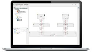
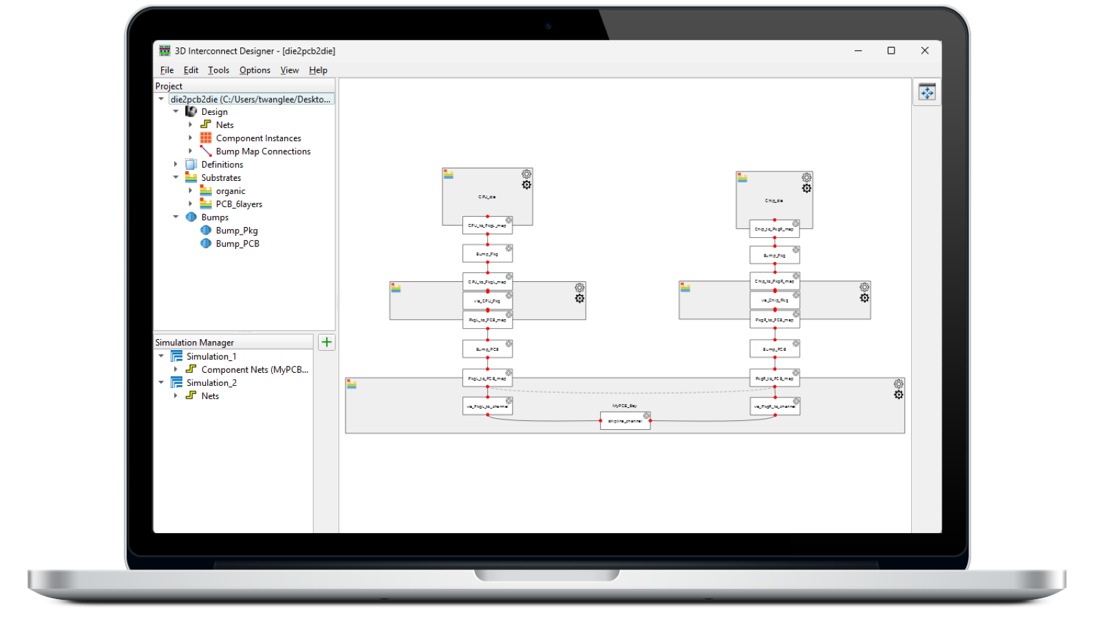
Accelerate Advanced Package & 3DIC Designs
Design, model, and validate complex 3D interconnect architectures with a powerful standalone design environment.

-
Scale AI Compute. Simplify Validation.
Automate transmitter and receiver validation across next-generation I/O, memory, and fabric interfaces.
-
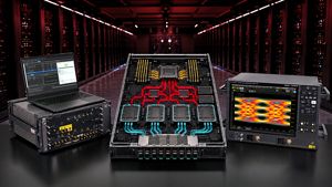
End-to-End Validation for AI Data Center
Strengthen 1.6T network reliability for AI-scale workloads from transceivers to interconnects.

-
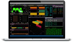
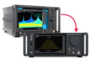
Take On Complex MIMO Signals
Pair Keysight VSA software with the new XA5 signal analyzer for advanced visualization, demodulation, and analysis — start your 30-day trial today.
-
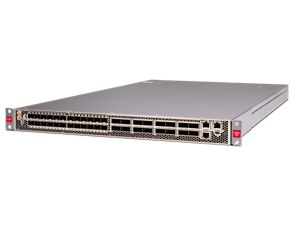
Introducing AI-Enhanced Packet Brokers
With extra memory and storage, these enhanced NPBs run Keysight's AI security and performance monitoring software and AI stack.
-
Accelerate Semiconductor Innovation
Explore end-to-end workflows spanning IC design, validation, wafer test, and photonics.

-
Trade In Before You Buy New
Save up to 50% on our latest instruments with eligible Keysight or competitor trade-ins.
-
448 Gb/s Waveform Generation
Achieve 200+ Gbaud multi-level modulated signals with high-speed AWGs for digital and optical standards.
-
The Right Connection Makes the Measurement
Maximize accuracy and performance with precision accessories engineered for Keysight instruments.

Trade In Before You Buy NewSave up to 50% on our latest instruments with eligible Keysight or competitor trade-ins.
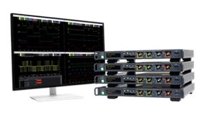
Scale to Hundreds of Channels. Keep Measurements in Sync.Four channels per 1U of rack space, up to 1 GHz bandwidth, and multi-oscilloscope synchronization.
-
-
Purpose-built solutions engineered for the design and test challenges unique to your industry.
Use Cases mapped to every stage of your product lifecycle, from design through operations.
Success Stories
Nokia + Keysight: AI Network Designs at Scale -
Authoritative application notes, data sheets, reference designs, and test procedures to accelerate design and validation decisions.
FeaturedHands‑on bootcamps that teach system design, test methods, and production workflows engineers can apply immediately.
Learning Hub
AI TechnologyExplore methodologies, test strategies, and technical resources for designing, validating, and scaling AI systems and networks.
-
Quick access to support related self-help tasks.
Additional content to support your product needs.
Do more with Keysight ServicesExplore services to accelerate every step of your innovation journey.






Measurement Probes Side Channel Analysis
Model: DS1203B
prev
- Overview
- Options
- Accessories
- Software
- Support
High Precision Electromagnetic Probe
The DS1203B High Precision Electromagnetic Probe, a highly precise probe used in side channel analysis, picks up electromagnetic emissions from semiconductor circuits.


-
Bandwidth
Up to 6 GHz
-
Technology
Device Security
-
Connector type
BNC / SMB
-
Product type
High precision electromagnetic probe
Ready for a quote
Find out what's included and explore available upgrade options from Keysight.
Highlights
The High Precision Electromagnetic Probe, a highly sensitive probe used in side channel analysis, picks up electromagnetic emissions from semiconductor circuits. The probe has a mechanism that allows you to swap out three different probe tips of varying sizes: 0.2 mm, 0.5 mm, and 1.25 mm. All tips have a directed coil and a protective Teflon shell. Normally used in combination with an XYZ-motion platform, the probe can pick up electromagnetic fields with frequencies of up to 6 GHz, converting them into an AC signal.
By moving over the surface of a target, the DS1203B can find highly active circuits, or hotspots. The signals picked up on a hotspot comprise the measurements for simple or differential electromagnetic analysis. The High Precision Electromagnetic Probe has a variable gain mechanism, which you can set by hand or through an external device and can vary based on the target’s characteristics.
Now includes New and improved Amplifier Unit
Services and support
Innovate at speed with curated support plans and prioritized response and turn-around times.
Get predictable, lease-based subscriptions and full lifecycle management solutions—so you reach your business goals faster.
Experience elevated service as a KeysightCare subscriber to get committed technical response and more.
Ensure your test system performs to specification and meets local and global standards.
Make measurements quickly with in-house, instructor-led training, and eLearning.
Download Keysight software or update your software to the newest version.
Frequently Asked Questions
Start your quote by choosing a product
Select a configuration below