Choose a country or area to see content specific to your location

데이터 시트
Features
Description
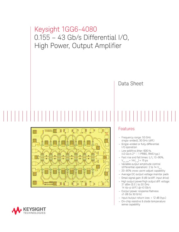
The 1GG6-4080 High Power, Differential I/O Amplifier is ideally suited as a MZ or LiNO3 Optical Modulator Driver for 10 & 43 Gb/s (NRZ OC-192 & OC-768) communication infrastructure and line-card amplification applications. Each fully differential I/O, integrated circuit is capable of amplifying high-speed clock and data signals with low additive jitter (< 600 fs RMS, PRBS) and fast edge speeds (~15 ps, 10–90% tr/tf).
These devices are fabricated using Keysight Technologies, Inc. PH9B GaAs PHEMT process to deliver ~8 dB differential small signal gain with up to 21 dBm S.E. Psat up to 30 GHz. On-chip bias capabilities allow for variable output amplitude control, cross-point control, monitoring of average DC output voltages and on-chip temperature.
Applications
The 1GG6-4080 can be used in a variety of high output power, frequency-domain applications through 30 GHz or high-speed time-domain applications requiring good pulse fidelity and high output voltage swings through 43 Gb/s. The device is ideal as a differential I/O, LiNO3 Optical Modulator Driver Amplifier for 10 & 43 Gb/s (NRZ OC-192 & OC-768) communication line card applications.
Biasing and Operation
The device consists of ground referenced, multi–section, cascoded differential amplifier stage. The subscripts “A” & “B” listed in the following voltage descriptions refer to the two sides of the differential structure. VG1A&B are the negative voltages applied to the common source FET gate networks of all cascoded stages; “A” along one side and “B” along the other side of the device. The VG1A&B voltages may be varied to accommodate a wide range of common–mode input voltages, typically 3.75 to 0 volts. VG2A&B are the negative voltages applied to the upper or second FET gates of all cascoded stages. VSS is the negative source voltage bias applied to all cascode FET source contacts. The drains of all cascoded FET sections are terminated to the chip backside providing a “ground reference” design for improved pulse fidelity performance. Typical bias conditions are as follows: VG1A&B = –17 volts, VG2A&B = –7.5 volts, and VSS adjusted to 300 mA ISS (typically VSS = –12.5 volts). For proper turn–on bias sequencing, the VG1 first gate voltages should be applied first, followed by the VG2 second gate voltages and then the VSS source voltages. For turn–off, the reverse sequence should be followed.
DC ground connections to the chip top–side GND contact pads are NOT required due to the conductive backside ground vias available on the MMIC. Conductive die-attach is required.
The provided “Absolute Maximum” specification limits have been determined such that the safe operating region and recommended maximum channel temperature (150 ºC) are not exceeded when the backside of the device is ≤ 75 ºC. Operating this device beyond the specified maximum voltage and current limits may result in rapid performance degradation or permanent damage to the device due to electrical overstress.
The chip also includes optional temperature monitoring contact pads for either a diode-based or resistor-based temperature sensing structures.
Assembly Techniques
GaAs MMICs are ESD sensitive. ESD preventive measures must be employed in all aspects of storage, handling, and assembly.
MMIC ESD precautions, handling considerations, die attach and bond- ing methods are critical factors in successful GaAs MMIC performance and reliability.
The Keysight Technologies, Inc. application note GaAs MMIC ESD, Die Attach and Bonding Guidelines, literature number 5991-3484EN, provides basic information on these subjects.
×
판매 문의 부탁드립니다.
*Indicates required field
감사합니다!
A sales representative will contact you soon.