Choose a country or area to see content specific to your location
What are you looking for?
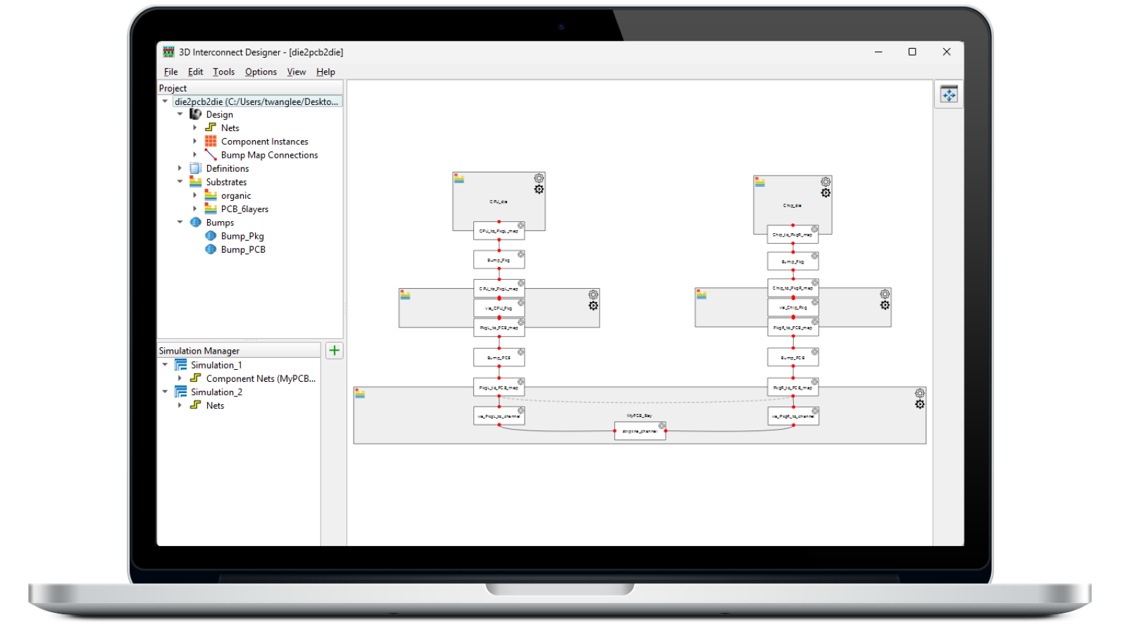
Design, model, and validate complex 3D interconnect architectures with a powerful standalone design environment.
Automate transmitter and receiver validation across next-generation I/O, memory, and fabric interfaces.
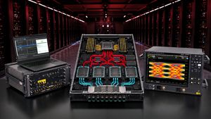
Strengthen 1.6T network reliability for AI-scale workloads from transceivers to interconnects.

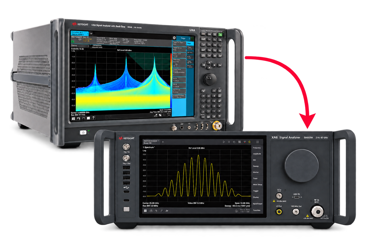
Pair Keysight VSA software with the new XA5 signal analyzer for advanced visualization, demodulation, and analysis — start your 30-day trial today.
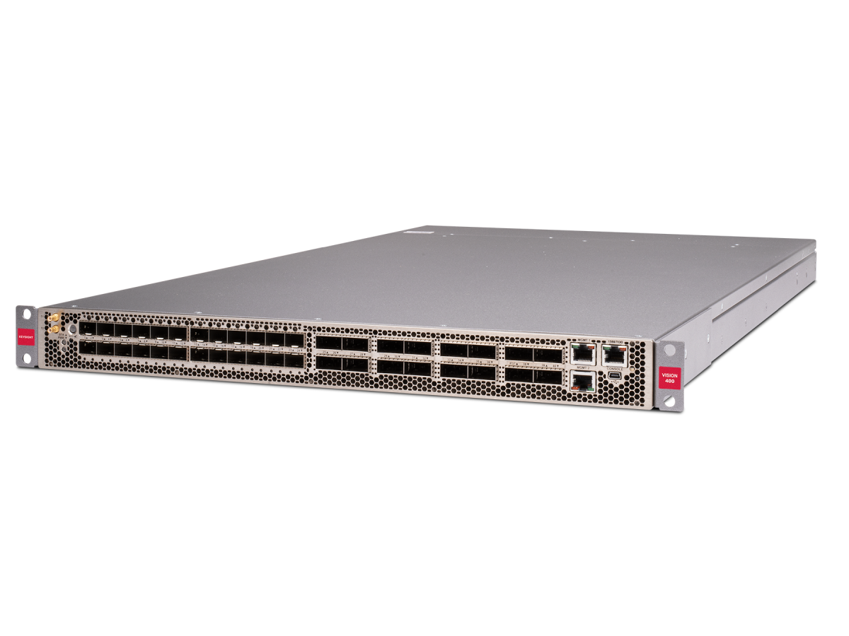
With extra memory and storage, these enhanced NPBs run Keysight's AI security and performance monitoring software and AI stack.
Explore end-to-end workflows spanning IC design, validation, wafer test, and photonics.
Save up to 50% on our latest instruments with eligible Keysight or competitor trade-ins.
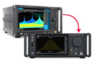
Achieve 200+ Gbaud multi-level modulated signals with high-speed AWGs for digital and optical standards.
Maximize accuracy and performance with precision accessories engineered for Keysight instruments.
Save up to 50% on our latest instruments with eligible Keysight or competitor trade-ins.
Four channels per 1U of rack space, up to 1 GHz bandwidth, and multi-oscilloscope synchronization.
Purpose-built solutions engineered for the design and test challenges unique to your industry.
Use Cases mapped to every stage of your product lifecycle, from design through operations.
Success Stories
Authoritative application notes, data sheets, reference designs, and test procedures to accelerate design and validation decisions.
Hands‑on bootcamps that teach system design, test methods, and production workflows engineers can apply immediately.
Learning Hub
Explore methodologies, test strategies, and technical resources for designing, validating, and scaling AI systems and networks.
Quick access to support related self-help tasks.
Additional content to support your product needs.
Explore services to accelerate every step of your innovation journey.
Turnkey solutions for device modeling and characterizing CMOS, RF, and III-V devices.
Accelerate PDK delivery with a proven end-to-end modeling platform.
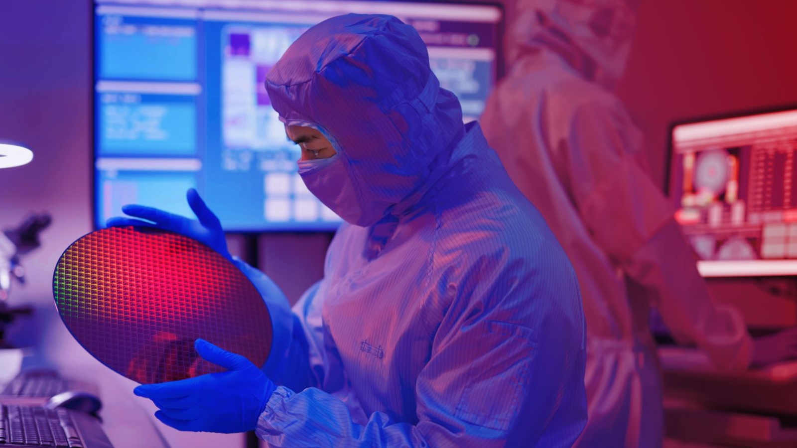
Leading foundries, IDMs, and fabless semiconductor companies rely on Keysight to transform measurement data into production-ready SPICE models. The Keysight Device Modeling Suite combines industry-standard characterization, extraction, validation, and noise analysis solutions into a unified workflow that shortens model development cycles and improves model quality.
With decades of device modeling expertise, support for advanced CMOS, RF, GaN, and power technologies, and a proven ecosystem trusted across the semiconductor industry, Keysight helps engineering teams deliver accurate, scalable, and designer-ready models with confidence.
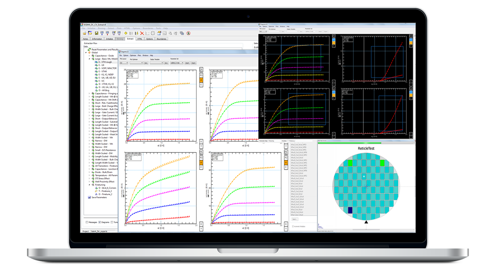
IC-CAP is the most advanced platform for semiconductor device modeling and characterization, trusted by foundries and fabless companies worldwide.
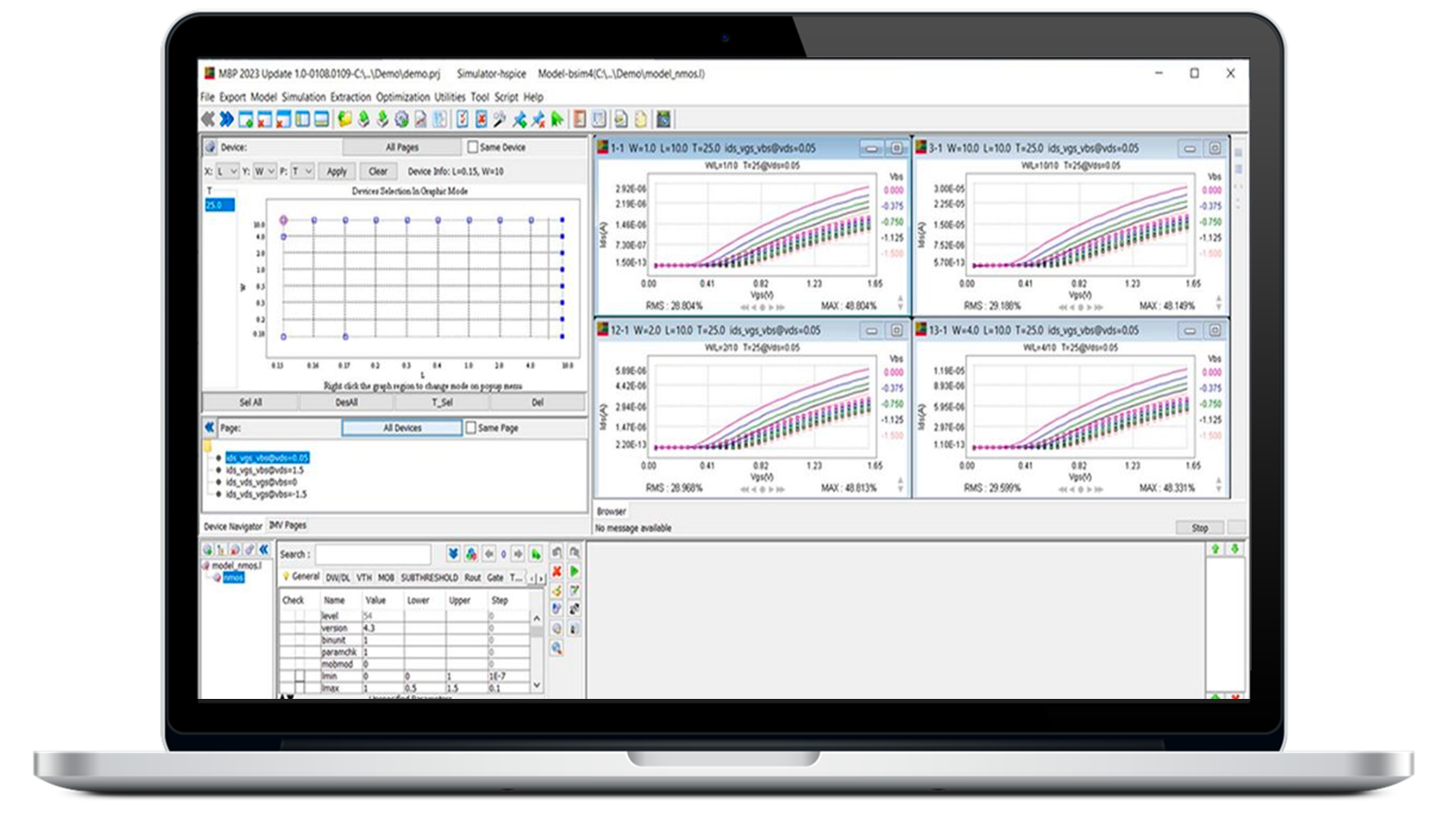
Model Builder Program (MBP) is a comprehensive solution for high-volume model generation, combining automation, flexibility, and accuracy.
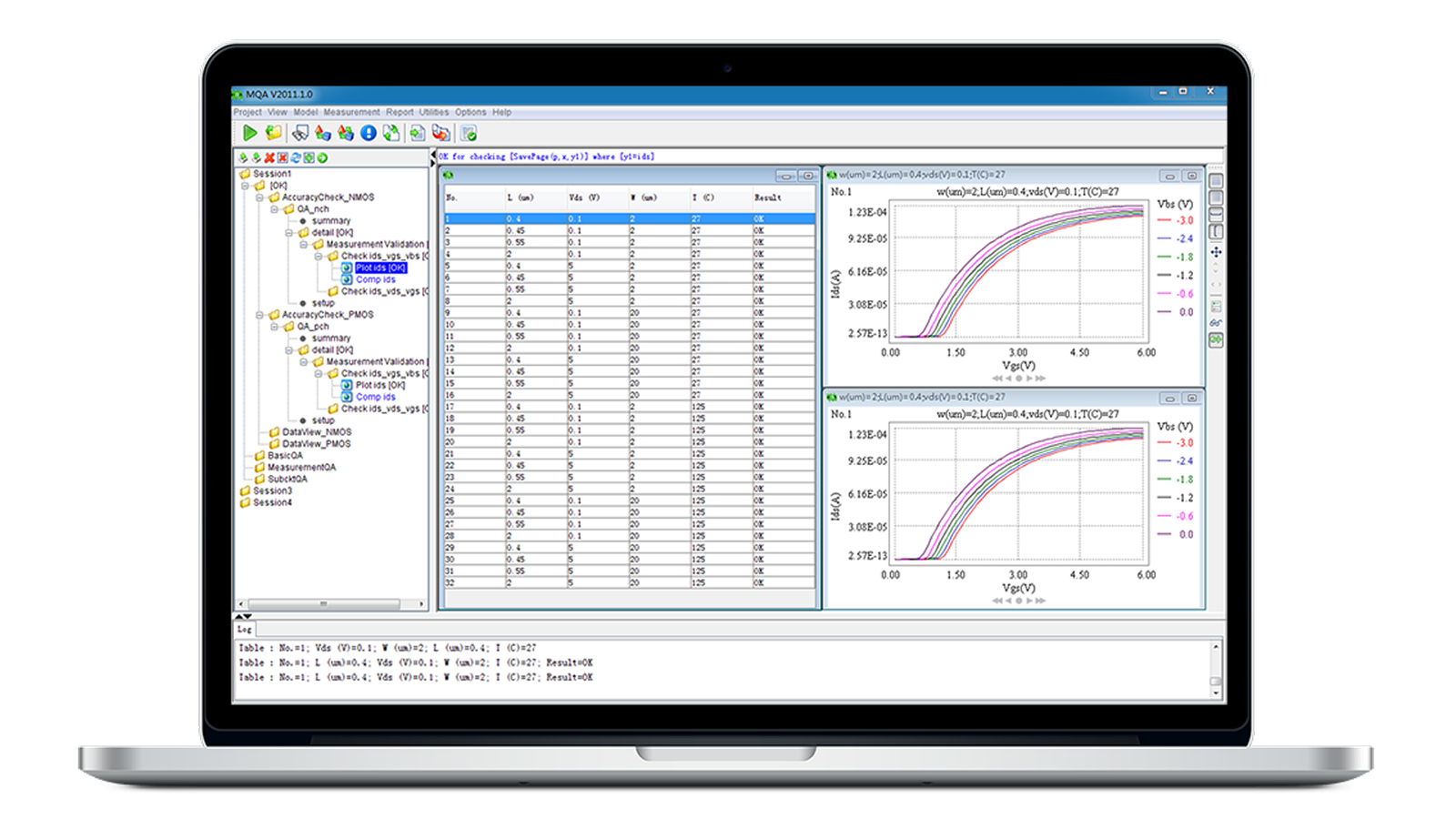
Device Modeling MQA is an industry standard, automated SPICE model validation software.
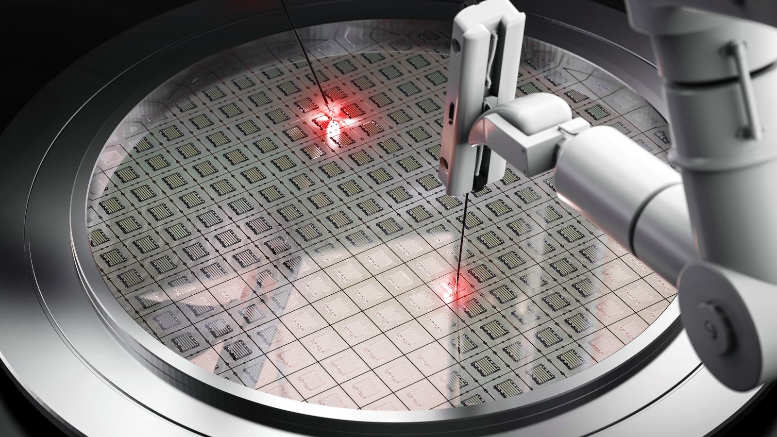
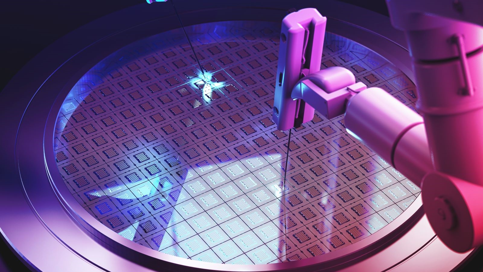
WaferPro Express software performs automated wafer-level measurements of semiconductor devices such as transistors and circuit components.
A-LFNA supports on-wafer measurement and analysis of low-frequency noise including flicker noise and random telegraph noise.
The semiconductor industry is at a massive inflection point. On one hand, devices featuring trillions of transistors and wide bandgap semiconductors are making waves across the electronic design industry. The combination of exploding volume of data and more complex models significantly increases pressure to meet time-to-market expectations. On the other hand, regional initiatives such as the CHIPS Act create unprecedented demand and growth opportunities. Foundry leaders will need to focus strategically on modernizing workflows to boost productivity and unlock areas of opportunity. Keysight EDA is at the forefront of this shift, working in close collaboration with foundries to deliver high quality models and PDKs tailored for Si, SiGe, GaAs, InP, and GaN processes. Our software and services form a total solution covering test structure design, device characterization and modeling, PDK creation, validation, and process and data management. Partner with Keysight EDA to innovate faster and smarter beyond Moore’s Law.
Traditional modeling approaches are increasingly challenged by the complexity, scale, and speed required in modern design environments. From neural network-based models that eliminate the need for manual parameter tuning to hybrid neural network architectures that blend physical insight with data-driven adaptability and ML-powered modeling workflows, these technologies enable faster, more accurate, and more scalable modeling solutions.
The applications and benchmarks presented demonstrate that AI/ML-based modeling not only improves predictive accuracy across DC, RF, and large-signal regimes but also reduces development time, enhances generalization across device variants, and lowers the barrier to entry for model developers.
Case Studies
Japan's National Institute of Advanced Industrial Science and Technology (AIST) successfully the measurements of random telegraph noise (RTN) in short-channel MOSFETs at cryogenic temperatures using the Keysight E4727B Advanced Low-Frequency Noise Analyzer is expanding the understanding of noise sources in quantum computing, paving the way for faster machines moving forward.
Case Studies
In a recent interview, Dr. Sadayuki Yoshitomi, Keysight Certified Expert (KCE), shared the challenges in high-speed NAND flash memory modeling and how KIOXIA accelerates PDK development by using Keysight's device modeling solution.
Case Studies
In recent years, Fin Field-Effect Transistors (FinFETs) have generated much interest, not only for digital applications, but also for RF solutions. Hangzhou Dianzi University created a novel compact model for bulk FinFETs that accommodates self-heating behaviors. Keysight Technologies’ IC-CAP software was used to accurately extract the necessary model parameters. In Figure 1, the simulation results of the model with self-heating effect (SHE) show excellent agreement with measurements up to 50.2 GHz.
Case Studies
Gallium nitride-based RF and power devices have gained tremendous momentum in recent years for next-generation communication like 5G and power electronic applications. Remarkable device properties such as high breakdown voltage, charge density, mobility, and saturation velocity increasingly enable improved performance for both RF and power circuits. To extract the best circuit-level performance from these devices in a time and cost-effective manner, advanced simulations and modeling capabilities are necessary.
Case Studies
The Keysight E4727B Advanced Low-Frequency Noise Analyzer (A-LFNA) enables non-destructive reliability characterization by leveraging 1/f noise measurements to reveal underlying device degradation mechanisms. This case study highlights research conducted at Imec on IGZO thin-film transistors and advanced Gate-All-Around nanosheet devices.
Case Studies
Accurate compact models are essential for reliable RF circuit design, but conventional GaAs pHEMT modeling workflows are often time-consuming, expertise-dependent, and difficult to maintain across wide operating conditions. Analog Devices, Inc. (ADI) collaborated with Keysight to address these challenges using an intelligent modeling solution that combines Machine Learning (ML)-driven automated parameter extraction with a hybrid Artificial Neural Network (ANN)-enhanced ASM-HEMT compact model.
Case Studies
Tohoku University in Japan is a major researcher of Tunnel Magneto-resistive (TMR) sensors. Their research is to develop novel materials and devices utilizing quantum spintronics. They are developing brain magnetic field sensing elements, spintronics-type quantum computing, and ultra-compact MRI system. As TMR sensors become more sensitive, it will be possible to detect even weak bio magnetic fields. The ultra-low noise TMR sensors are not only for biological signal applications, but it will dramatically be expanding the range of applications. Keysight E4727B Advanced Low-Frequency Noise Analyzer is an important solution for them.
See how the Machine Learning Optimizer in Device Modeling MBP dramatically improves modeling efficiency by automating and simplifying complex workflows.
Learn about the best practices for RTN detection, large data post-processing, remote control, and integration into reliability workflows.
White Papers
Product Fact Sheets
Product Fact Sheets
Discover the latest release designed to help engineers work faster, simulate more accurately, and accelerate product development.
Device modeling creates mathematical representations of semiconductor devices that predict electrical behavior under varying operating conditions, enabling accurate simulation and design optimization before hardware fabrication.
The solutions support a wide range of technologies, including CMOS, bipolar, GaAs, GaN, RF, compound semiconductor, and wide-bandgap devices used in advanced electronic and photonic applications.
Device characterization captures measured electrical data across operating conditions, providing the foundation for parameter extraction and ensuring models closely represent real device behavior.
Yes. Automated extraction, validation, and model quality assurance workflows help reduce modeling effort, improve consistency, and speed the delivery of high-quality PDKs.
Model validation verifies that extracted models remain accurate across bias, geometry, temperature, and frequency ranges, ensuring reliable circuit simulation and design results.
Talk to our team to find the right solution for your design needs, get a personalized quote, or request a free trial.
What are you looking for?