


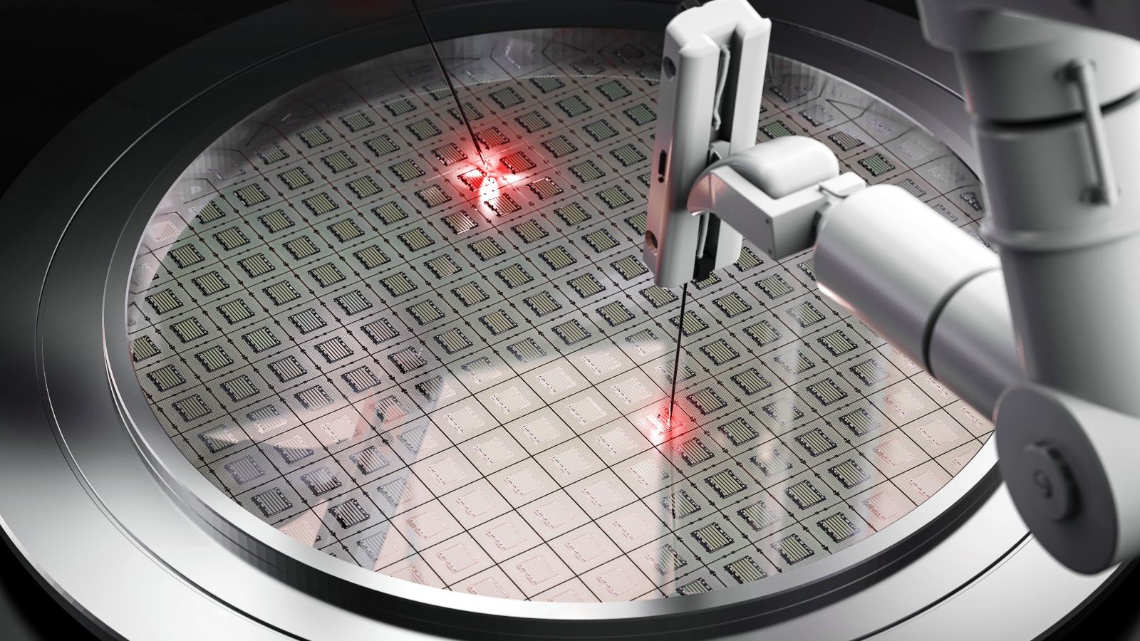
Why Choose Keysight Device Modeling Suite
Accelerate PDK delivery with a proven end-to-end modeling platform.
Leading foundries, IDMs, and fabless semiconductor companies rely on Keysight to transform measurement data into production-ready SPICE models. The Keysight Device Modeling Suite combines industry-standard characterization, extraction, validation, and noise analysis solutions into a unified workflow that shortens model development cycles and improves model quality.
With decades of device modeling expertise, support for advanced CMOS, RF, GaN, and power technologies, and a proven ecosystem trusted across the semiconductor industry, Keysight helps engineering teams deliver accurate, scalable, and designer-ready models with confidence.
Integrated Circuit Characterization and Analysis Program (IC-CAP)
IC-CAP is the most advanced platform for semiconductor device modeling and characterization, trusted by foundries and fabless companies worldwide.
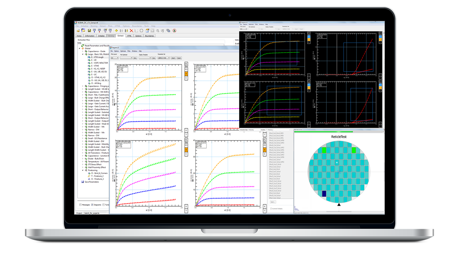
Model Builder Program (MBP)
Model Builder Program (MBP) is a comprehensive solution for high-volume model generation, combining automation, flexibility, and accuracy.
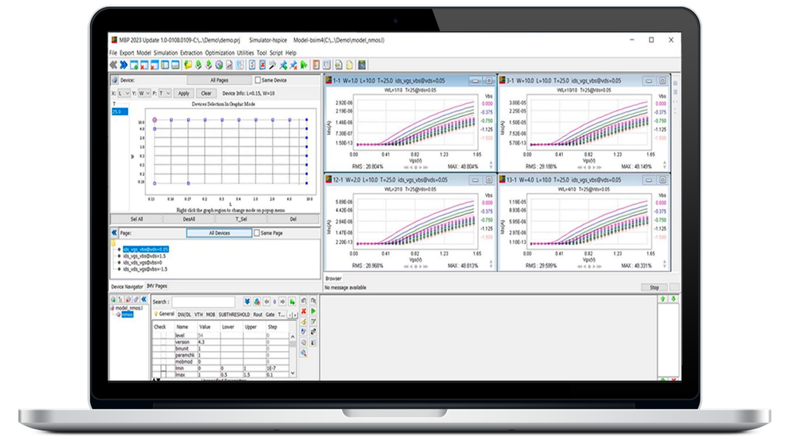
Model Quality Assurance (MQA)
Device Modeling MQA is an industry standard, automated SPICE model validation software.
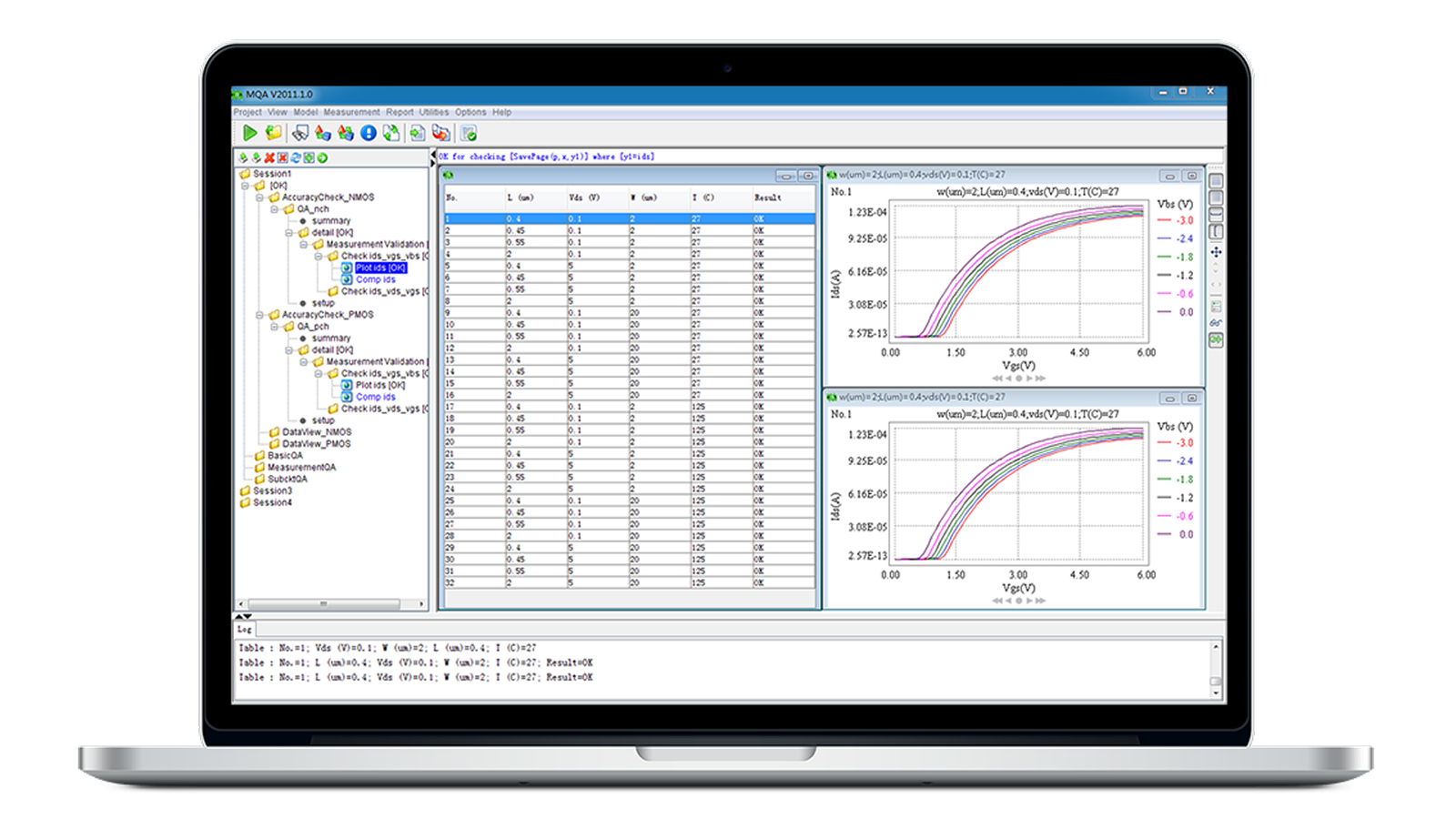
WaferPro Express
WaferPro Express software performs automated wafer-level measurements of semiconductor devices such as transistors and circuit components.

Advanced Low-Frequency Noise Analyzer (A-LFNA)
A-LFNA supports on-wafer measurement and analysis of low-frequency noise including flicker noise and random telegraph noise.



Keysight EDA Solutions for Semiconductor Foundries
The semiconductor industry is at a massive inflection point. On one hand, devices featuring trillions of transistors and wide bandgap semiconductors are making waves across the electronic design industry. The combination of exploding volume of data and more complex models significantly increases pressure to meet time-to-market expectations. On the other hand, regional initiatives such as the CHIPS Act create unprecedented demand and growth opportunities. Foundry leaders will need to focus strategically on modernizing workflows to boost productivity and unlock areas of opportunity. Keysight EDA is at the forefront of this shift, working in close collaboration with foundries to deliver high quality models and PDKs tailored for Si, SiGe, GaAs, InP, and GaN processes. Our software and services form a total solution covering test structure design, device characterization and modeling, PDK creation, validation, and process and data management. Partner with Keysight EDA to innovate faster and smarter beyond Moore’s Law.
Accelerating Semiconductor Innovation through Machine Learning-Driven Device Modeling
Traditional modeling approaches are increasingly challenged by the complexity, scale, and speed required in modern design environments. From neural network-based models that eliminate the need for manual parameter tuning to hybrid neural network architectures that blend physical insight with data-driven adaptability and ML-powered modeling workflows, these technologies enable faster, more accurate, and more scalable modeling solutions.
The applications and benchmarks presented demonstrate that AI/ML-based modeling not only improves predictive accuracy across DC, RF, and large-signal regimes but also reduces development time, enhances generalization across device variants, and lowers the barrier to entry for model developers.


Resources to Get You Started
See how the Machine Learning Optimizer in Device Modeling MBP dramatically improves modeling efficiency by automating and simplifying complex workflows.


Learn about the best practices for RTN detection, large data post-processing, remote control, and integration into reliability workflows.
BOOTCAMPS
AI/ML Innovations in Device Modeling

BOOTCAMPS
Semiconductor Device Noise Measurements
White Papers
Accelerating Semiconductor Innovation through Machine Learning-Driven Modeling

Configuration Guides
Device Modeling MBP Configuration
Product Fact Sheets
Keysight EDA Platform OS Support Roadmap MBPMQA
Product Fact Sheets
Keysight EDA Platform OS Support Roadmap
Have Questions? We've Got Answers
Device modeling creates mathematical representations of semiconductor devices that predict electrical behavior under varying operating conditions, enabling accurate simulation and design optimization before hardware fabrication.
The solutions support a wide range of technologies, including CMOS, bipolar, GaAs, GaN, RF, compound semiconductor, and wide-bandgap devices used in advanced electronic and photonic applications.
Device characterization captures measured electrical data across operating conditions, providing the foundation for parameter extraction and ensuring models closely represent real device behavior.
Yes. Automated extraction, validation, and model quality assurance workflows help reduce modeling effort, improve consistency, and speed the delivery of high-quality PDKs.
Model validation verifies that extracted models remain accurate across bias, geometry, temperature, and frequency ranges, ensuring reliable circuit simulation and design results.