How to Perform On-Wafer Device Characterization at Sub-THz Frequencies

Sub-THz Device Characterization
On-wafer characterization at sub-terahertz frequencies requires broadband measurements that isolate the intrinsic electrical behavior of semiconductor devices from the influence of probes, interconnects, and measurement fixtures. The measurement configuration includes a vector network analyzer, broadband frequency extenders, a test set controller, precision calibration substrates, and ground-signal-ground wafer probes operating across wide frequency ranges. Engineers perform calibrated broadband scattering parameter measurements directly on semiconductor wafers to evaluate active and passive devices before packaging. Typical devices include transimpedance amplifiers, electro-optical drivers, monolithic microwave integrated circuits, differential amplifiers, and emerging sub-terahertz components for optical communications, sensing, and artificial intelligence hardware.
The acquired measurement data is used to validate circuit performance, extract compact device models, and compare measured electrical behavior against electromagnetic and circuit simulations. Broadband measurements provide insight into gain, isolation, impedance matching, bandwidth, stability, and differential operation while maintaining a consistent calibration across the entire measurement range. By performing characterization before packaging, engineers can identify process variations, optimize device layouts, verify design assumptions, and accelerate design iterations without the additional uncertainty introduced by packages or external interconnect structures.

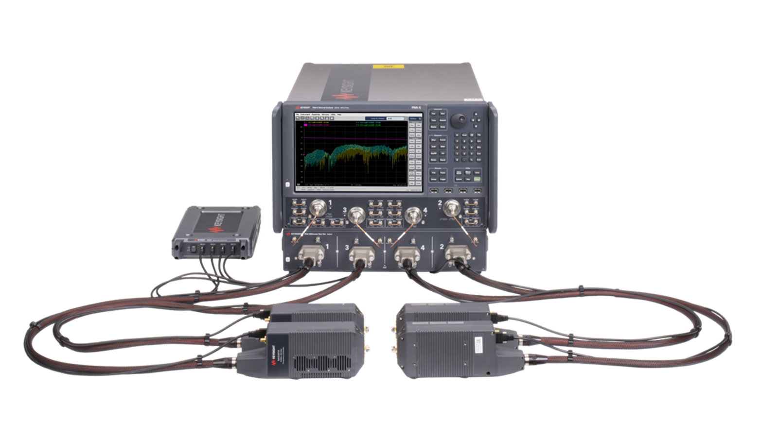
Sub-THz Device Characterization Solution
See Block Diagram of Sub-THz Device Characterization Solution


Explore Products in Our Sub-THz Device Characterization Solution
-

![]()
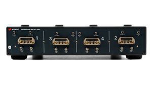
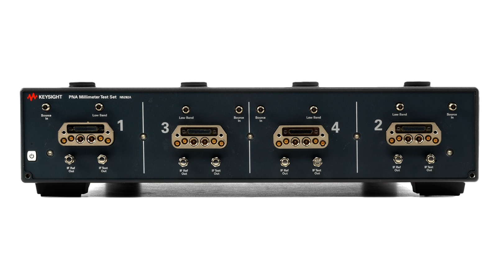
N5292A Millimeter-wave Test Set Controller for PNA/PNA-X Network Analyzer Series, 2- or 4-port
-
![]()
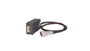
NA5307A Frequency Extender, 250 GHz
-
![]()
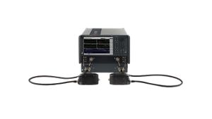
N5290A PNA Millimeter Wave System


Discover Resources and Insights
Additional Resources for Sub-THz Device Characterization
Related Use Cases


-
![]()
Learn More
How to Characterize Materials for High-Frequency Electronic Designs
Characterize dielectric and conductive materials using a vector network analyzer and resonator measurement techniques.
Learn More

-
![]()
Learn More
How to Measure Power Rail Ripple
Learn how to measure ripple and noise on DC power rails with a low-noise oscilloscope setup, a dedicated power rail probe, and loading-aware techniques that keep measurement-induced distortion low.
Learn More
-
![]()
Learn More
How to Compare Low-Pass, High-Pass, and Band-Pass Filter Response
Comparing how low-pass, high-pass, and band-pass circuits shape gain and phase across frequency requires an Essential benchtop oscilloscope. Learn how to compare filters using oscilloscopes with built-in waveform generation and Bode-plot measurements.
Learn More

Get in Touch with One of Our Experts
Need help finding the right solution for you?