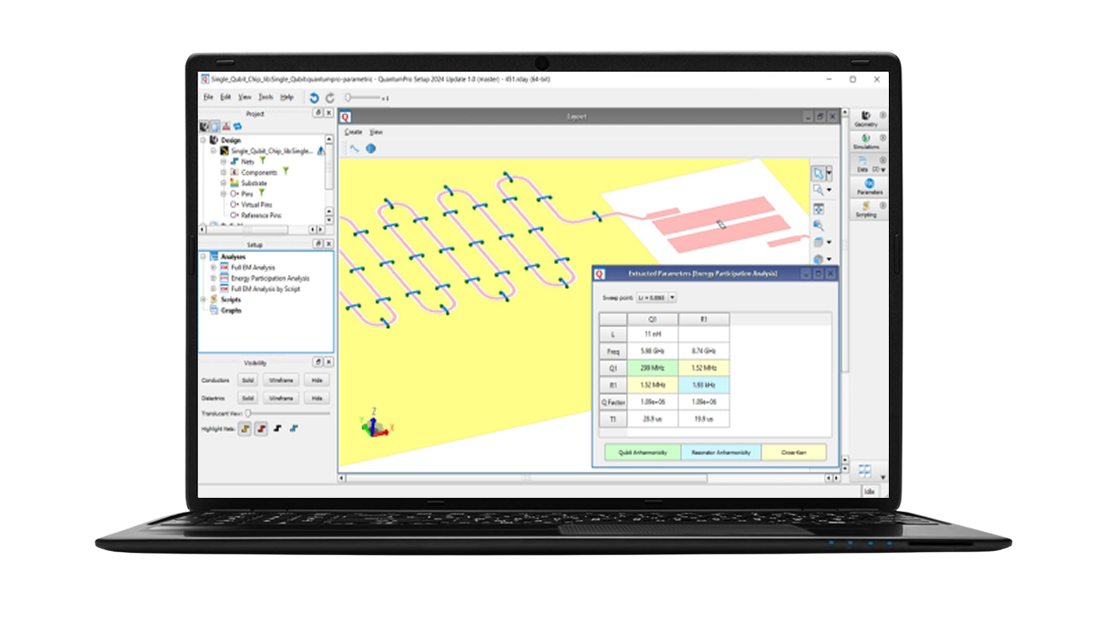
Choose a country or area to see content specific to your location
What are you looking for?
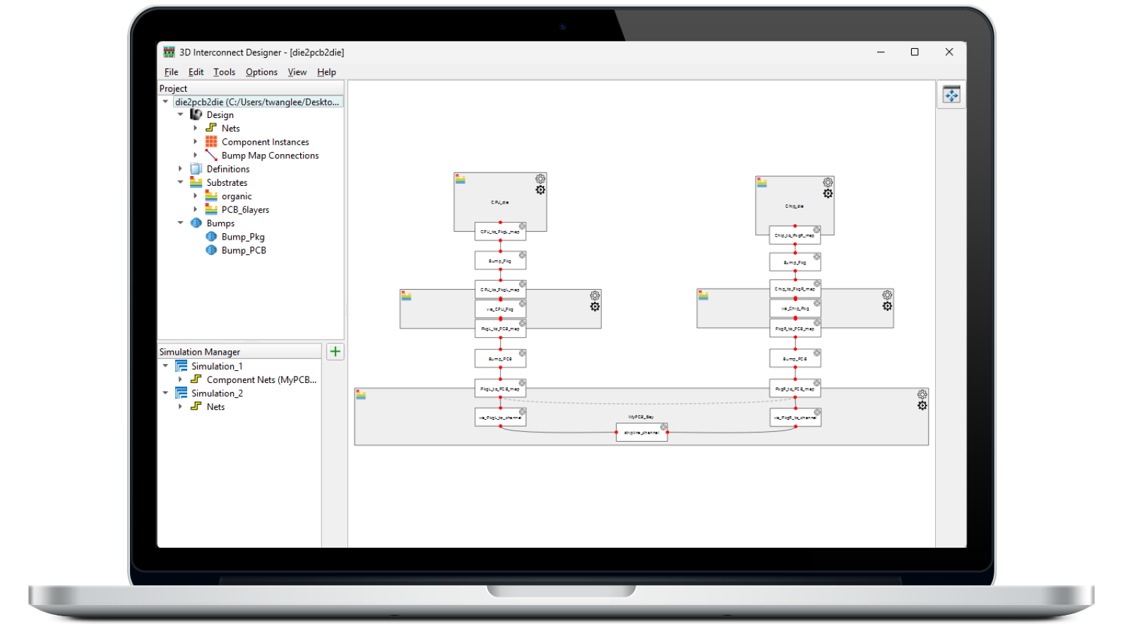
Design, model, and validate complex 3D interconnect architectures with a powerful standalone design environment.
Automate transmitter and receiver validation across next-generation I/O, memory, and fabric interfaces.
Strengthen 1.6T network reliability for AI-scale workloads from transceivers to interconnects.

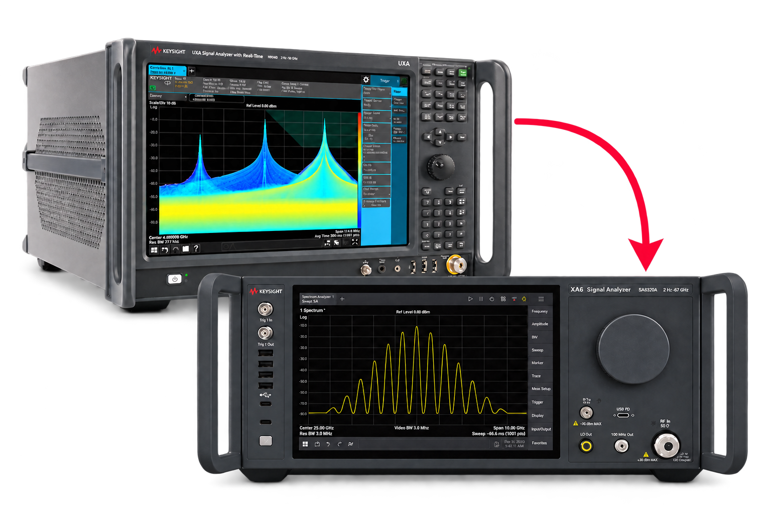
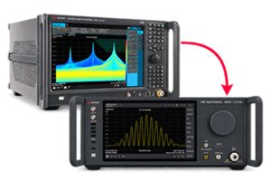
Pair Keysight VSA software with the new XA5 signal analyzer for advanced visualization, demodulation, and analysis — start your 30-day trial today.
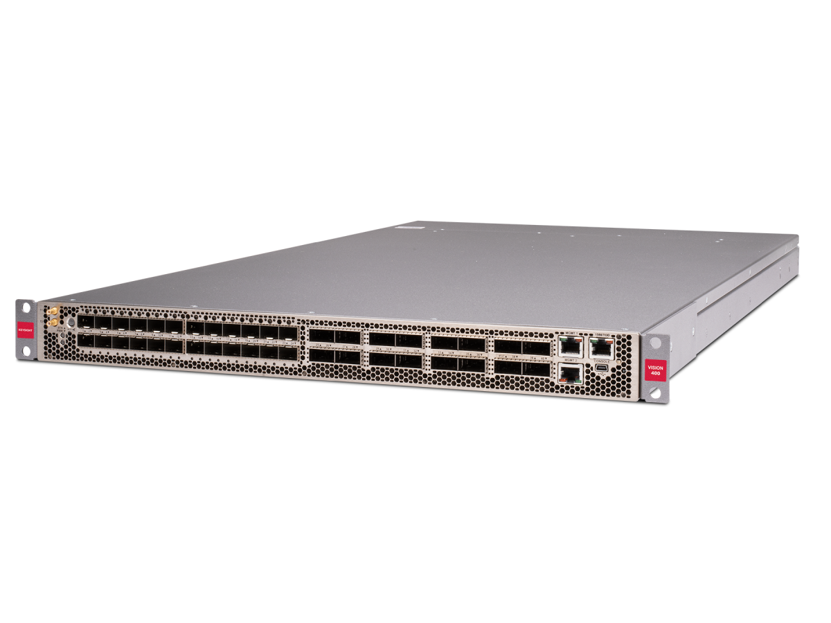
With extra memory and storage, these enhanced NPBs run Keysight's AI security and performance monitoring software and AI stack.
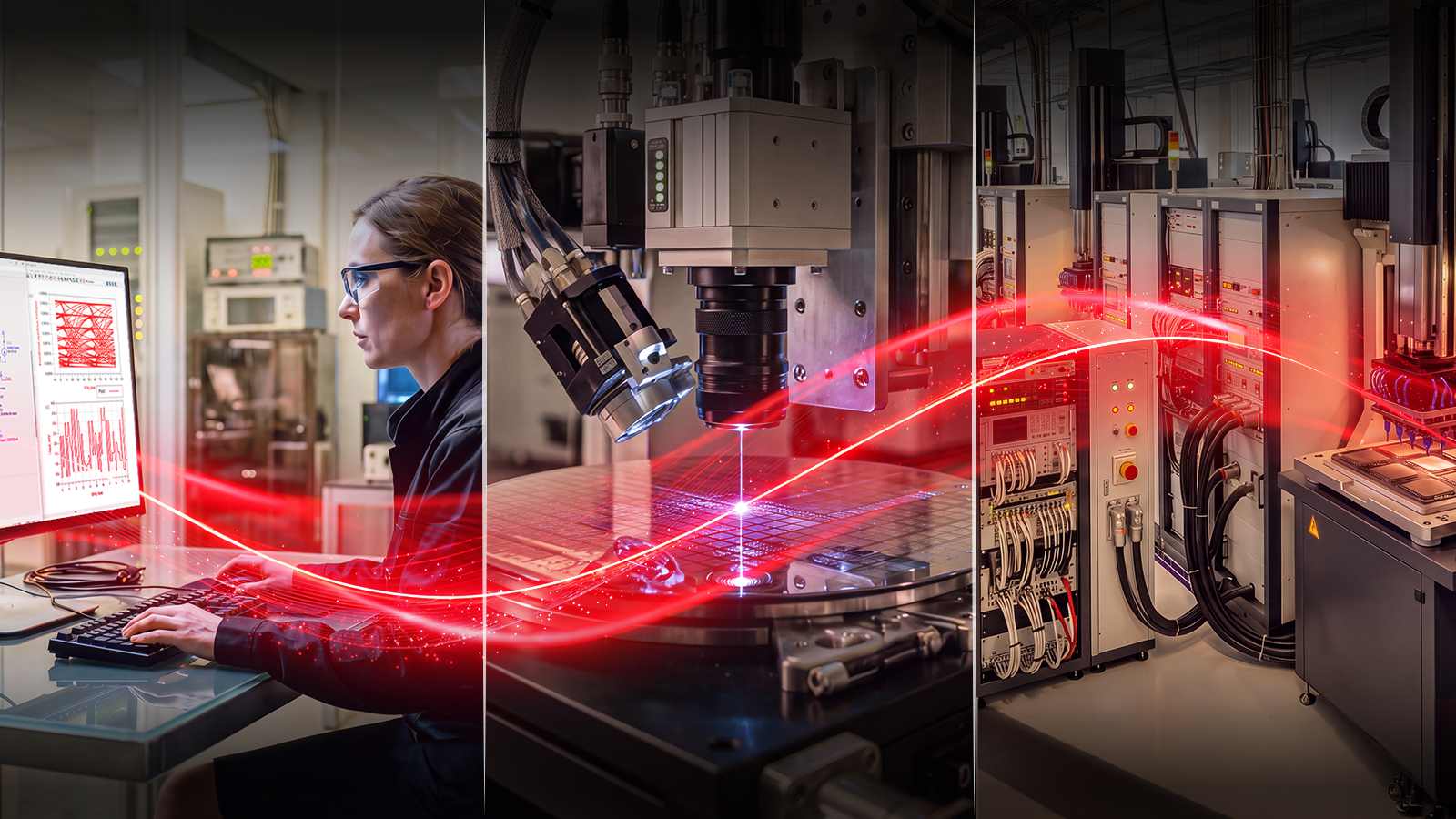
Explore end-to-end workflows spanning IC design, validation, wafer test, and photonics.

Save up to 50% on our latest instruments with eligible Keysight or competitor trade-ins.
Achieve 200+ Gbaud multi-level modulated signals with high-speed AWGs for digital and optical standards.
Maximize accuracy and performance with precision accessories engineered for Keysight instruments.
Save up to 50% on our latest instruments with eligible Keysight or competitor trade-ins.
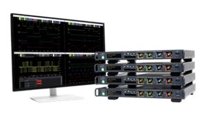
Four channels per 1U of rack space, up to 1 GHz bandwidth, and multi-oscilloscope synchronization.
Purpose-built solutions engineered for the design and test challenges unique to your industry.
Use Cases mapped to every stage of your product lifecycle, from design through operations.
Success Stories
Authoritative application notes, data sheets, reference designs, and test procedures to accelerate design and validation decisions.
Hands‑on bootcamps that teach system design, test methods, and production workflows engineers can apply immediately.
Learning Hub
Explore methodologies, test strategies, and technical resources for designing, validating, and scaling AI systems and networks.
Quick access to support related self-help tasks.
Additional content to support your product needs.
Explore services to accelerate every step of your innovation journey.
EDA electromagnetic design environment for the seamless design of superconducting qubits.
EM in • Quantum out—automated quantum-parameter extraction.
QuantumPro connects layout and circuit design with electromagnetic simulation and quantum-parameter extraction. It supports finite-element frequency-domain and eigenmode analysis, method of moments (MoM) simulation, superconducting material modeling, including kinetic inductance, and Python-based design automation.
Electromagnetic (EM) simulation brings you insight before physical prototyping.
Integrated circuit/layout/EM for the design of superconducting qubits.
QuantumPro 3DEM simulators (FEM for frequency domain and eigenmode and Momentum for frequency domain).
Automated quantum parameter extraction from both frequency-domain and eigenmode solutions.
Linear Circuit Simulator for EM-circuit co-simulation.
Modeling of the kinetic inductance in the EM flow.
Revolutionize your workflow with automated quantum parameter extraction from both frequency-domain and eigenmode solutions. Effortlessly optimize with built-in design automation via ADS/QuantumPro Python scripting. Elevate your EM flow with kinetic inductance modeling. Experience quantum innovation simplified with QuantumPro.
How-To Videos
How-To Videos
Demos
Demos
Article Reprints
Application Notes
Application Notes
ADS software bundles provide designers with pre-configured combinations targeted to a specific design workflow.
W3704B ADS and EM design environments with linear circuit and QuantumPro — An integrated circuit, layout, EM, and quantum extraction workflow for the seamless design of superconducting qubits.
W3704B
W3704B ADS and EM design environments with linear circuit and QuantumPro — An integrated circuit, layout, EM, and quantum extraction workflow for the seamless design of superconducting qubits.
The W3704B ADS Core, EM Design, Layout, QuantumPro includes:
The W3704B ADS bundle offers an all-inclusive design environment for faster development of superconducting qubits, seamlessly combining circuit analysis (linear only), layout, EM, and quantum extraction in one integrated workflow. Empower your quantum designs with the specialized Quantum layout library. Precision is paramount with QuantumPro 3DEM simulators, spanning FEM for frequency domain and eigenmode, and Momentum for frequency domain analyses. Revolutionize your workflow with automated quantum parameter extraction from both frequency-domain and eigenmode solutions. Effortlessly optimize with built-in design automation via ADS/QuantumPro Python scripting. Elevate your EM flow with kinetic inductance modeling. Experience quantum innovation simplified with ADS.
W3706B ADS and EM design environments with Quantum Ckt Sim and QuantumPro — An integrated circuit, layout, EM, and quantum extraction workflow for the seamless design of both superconducting qubits and quantum amplifiers.
W3706B
W3706B ADS and EM design environments with Quantum Ckt Sim and QuantumPro — An integrated circuit, layout, EM, and quantum extraction workflow for the seamless design of both superconducting qubits and quantum amplifiers.
The W3706B ADS Core, EM Design Core, Layout, QuantumPro, Quantum Ckt Sim includes:
The W3706B ADS bundle offers an all-inclusive design environment for faster development of both superconducting qubits and quantum amplifiers, seamlessly combining circuit analysis (full capabilities including nonlinear), layout, EM, and quantum extraction in one integrated workflow. Empower your quantum designs with the specialized Quantum layout library. Precision is paramount with QuantumPro 3DEM simulators, spanning FEM for frequency domain and eigenmode, and Momentum for frequency domain analyses. Revolutionize your workflow with automated quantum parameter extraction from both frequency-domain and eigenmode solutions. Effortlessly optimize with built-in design automation via ADS/QuantumPro Python scripting. Elevate your EM flow with kinetic inductance modeling. Transform your quantum workflow with flux quantization in the frequency domain. You can feel confident with our accurate and reliable analysis for large, highly nonlinear quantum circuits.
W3715B ADS and EM design environments with nonlinear circuit and QuantumPro — An integrated circuit, layout, EM, and quantum extraction workflow for the seamless design of both superconducting qubits and quantum amplifiers.
W3715B
W3715B ADS and EM design environments with nonlinear circuit and QuantumPro — An integrated circuit, layout, EM, and quantum extraction workflow for the seamless design of both superconducting qubits and quantum amplifiers.
The W3715B ADS Core, EM Design Core, Layout, QuantumPro, HB includes:
The W3715B ADS bundle offers an all-inclusive design environment for faster development of both superconducting qubits and quantum amplifiers, seamlessly combining circuit analysis (including nonlinear), layout, EM, and quantum extraction in one integrated workflow. Empower your quantum designs with the specialized Quantum layout library. Precision is paramount with QuantumPro 3DEM simulators, spanning FEM for frequency domain and eigenmode, and Momentum for frequency domain analyses. Revolutionize your workflow with automated quantum parameter extraction from both frequency-domain and eigenmode solutions. Effortlessly optimize with built-in design automation via ADS/QuantumPro Python scripting. Elevate your EM flow with kinetic inductance modeling. Additionally, the nonlinear circuit environment provides deep insights into the power-dependent performance of your quantum chips through our market-leading nonlinear circuit design environment. Experience quantum innovation simplified with ADS.
Electromagnetic simulation is the process of modeling the electric and magnetic fields within superconducting quantum circuits and their surrounding structures. It enables engineers to predict how qubits, resonators, couplers, control lines, packages, and cavities interact before fabrication. By accurately characterizing electromagnetic behavior, designers can extract critical quantum parameters, identify unwanted modes, and optimize device performance early in the design cycle. QuantumPro from Keysight integrates EM simulation directly into the quantum design workflow to help accelerate superconducting qubit development.
Superconducting qubits are highly sensitive to their electromagnetic environment. Small changes in geometry, material properties, packaging, or interconnects can impact qubit frequencies, coupling strengths, coherence, and crosstalk. EM simulation enables designers to understand these effects before fabrication and optimize designs to minimize loss mechanisms and unwanted resonances. This helps improve qubit performance while reducing costly design iterations.
Modern quantum EM simulation tools can extract many of the parameters needed for quantum hardware design, including qubit frequencies, resonator frequencies, coupling coefficients, energy participation ratios (EPRs), capacitance matrices, inductance values, and mode structures. These parameters can then be passed to quantum circuit simulators and Hamiltonian-based analysis tools to predict device behavior with greater accuracy. QuantumPro provides integrated quantum parameter extraction as part of its EM-driven workflow.
Yes. Advanced quantum EM simulators can model complete 3D environments, including chip packages, cavities, interposers, wirebonds, connectors, and control-line structures. As quantum processors scale, packaging effects increasingly influence device performance through the introduction of unwanted resonances, crosstalk paths, and radiation losses. EM simulation allows engineers to analyze these interactions and optimize both the chip and package simultaneously. Keysight highlights support for full 3D modeling and simulation of qubits, cavities, and packaging within its quantum design environment.
EM simulation reduces the need for repeated fabrication cycles by enabling virtual prototyping of quantum devices. Engineers can evaluate multiple design alternatives, optimize layouts, identify performance bottlenecks, and verify electromagnetic behavior before manufacturing hardware. By combining EM analysis with circuit simulation and system-level quantum modeling, development teams can move more quickly from concept to validated design while improving confidence in device performance. This integrated approach is a key reason why EM simulation has become a foundational technology for scalable quantum computing development.
Talk to our team to find the right solution for your design needs, get a personalized quote, or request a free trial.
What are you looking for?