Learn More
segmentation:campaign/Bench,segmentation:product-category/AC_DC_Power_Sources_Loads,segmentation:product-category/AC_DC_Power_Sources_Loads/DC_Power_Supplies,segmentation:business-unit/EISG,keysight:product-lines/1h,segmentation:funnel/bofu,keysight:dtx/solutions/facets/development-area/power,keysight:dtx/solutions/facets/workflow-stage/functional-test,keysight:dtx/solutions/facets/industry/semiconductor,keysight:dtx/solutions/facets/design-and-test-product/power-supply,keysight:models/pz/pz2100a,keysight:models/pz/pz2131a,keysight:models/px/px0106a,keysight:models/px/px0103a,keysight:models/px/px0110a,keysight:models/n1/n1295a,keysight:models/pw/pw9251asegmentation:campaign/Bench,segmentation:product-category/AC_DC_Power_Sources_Loads,segmentation:product-category/AC_DC_Power_Sources_Loads/DC_Power_Supplies,segmentation:business-unit/EISG,keysight:product-lines/1h,segmentation:funnel/bofu,keysight:dtx/solutions/facets/development-area/power,keysight:dtx/solutions/facets/workflow-stage/functional-test,keysight:dtx/solutions/facets/industry/semiconductor,keysight:dtx/solutions/facets/design-and-test-product/power-supply,keysight:models/pz/pz2100a,keysight:models/pz/pz2131a,keysight:models/px/px0106a,keysight:models/px/px0103a,keysight:models/px/px0110a,keysight:models/n1/n1295a,keysight:models/pw/pw9251asegmentation:campaign/Bench,segmentation:product-category/AC_DC_Power_Sources_Loads,segmentation:product-category/AC_DC_Power_Sources_Loads/DC_Power_Supplies,segmentation:business-unit/EISG,keysight:product-lines/1h,segmentation:funnel/bofu,keysight:dtx/solutions/facets/development-area/power,keysight:dtx/solutions/facets/workflow-stage/functional-test,keysight:dtx/solutions/facets/industry/semiconductor,keysight:dtx/solutions/facets/design-and-test-product/power-supply,keysight:models/pz/pz2100a,keysight:models/pz/pz2131a,keysight:models/px/px0106a,keysight:models/px/px0103a,keysight:models/px/px0110a,keysight:models/n1/n1295a,keysight:models/pw/pw9251asegmentation:campaign/Bench,segmentation:product-category/AC_DC_Power_Sources_Loads,segmentation:product-category/AC_DC_Power_Sources_Loads/DC_Power_Supplies,segmentation:business-unit/EISG,keysight:product-lines/1h,segmentation:funnel/bofu,keysight:dtx/solutions/facets/development-area/power,keysight:dtx/solutions/facets/workflow-stage/functional-test,keysight:dtx/solutions/facets/industry/semiconductor,keysight:dtx/solutions/facets/design-and-test-product/power-supply,keysight:models/pz/pz2100a,keysight:models/pz/pz2131a,keysight:models/px/px0106a,keysight:models/px/px0103a,keysight:models/px/px0110a,keysight:models/n1/n1295a,keysight:models/pw/pw9251asegmentation:campaign/Bench,segmentation:product-category/AC_DC_Power_Sources_Loads,segmentation:product-category/AC_DC_Power_Sources_Loads/DC_Power_Supplies,segmentation:business-unit/EISG,keysight:product-lines/1h,segmentation:funnel/bofu,keysight:dtx/solutions/facets/development-area/power,keysight:dtx/solutions/facets/workflow-stage/functional-test,keysight:dtx/solutions/facets/industry/semiconductor,keysight:dtx/solutions/facets/design-and-test-product/power-supply,keysight:models/pz/pz2100a,keysight:models/pz/pz2131a,keysight:models/px/px0106a,keysight:models/px/px0103a,keysight:models/px/px0110a,keysight:models/n1/n1295a,keysight:models/pw/pw9251asegmentation:campaign/Bench,segmentation:product-category/AC_DC_Power_Sources_Loads,segmentation:product-category/AC_DC_Power_Sources_Loads/DC_Power_Supplies,segmentation:business-unit/EISG,keysight:product-lines/1h,segmentation:funnel/bofu,keysight:dtx/solutions/facets/development-area/power,keysight:dtx/solutions/facets/workflow-stage/functional-test,keysight:dtx/solutions/facets/industry/semiconductor,keysight:dtx/solutions/facets/design-and-test-product/power-supply,keysight:models/pz/pz2100a,keysight:models/pz/pz2131a,keysight:models/px/px0106a,keysight:models/px/px0103a,keysight:models/px/px0110a,keysight:models/n1/n1295a,keysight:models/pw/pw9251asegmentation:campaign/Bench,segmentation:product-category/AC_DC_Power_Sources_Loads,segmentation:product-category/AC_DC_Power_Sources_Loads/DC_Power_Supplies,segmentation:business-unit/EISG,keysight:product-lines/1h,segmentation:funnel/bofu,keysight:dtx/solutions/facets/development-area/power,keysight:dtx/solutions/facets/workflow-stage/functional-test,keysight:dtx/solutions/facets/industry/semiconductor,keysight:dtx/solutions/facets/design-and-test-product/power-supply,keysight:models/pz/pz2100a,keysight:models/pz/pz2131a,keysight:models/px/px0106a,keysight:models/px/px0103a,keysight:models/px/px0110a,keysight:models/n1/n1295a,keysight:models/pw/pw9251asegmentation:campaign/Bench,segmentation:product-category/AC_DC_Power_Sources_Loads,segmentation:product-category/AC_DC_Power_Sources_Loads/DC_Power_Supplies,segmentation:business-unit/EISG,keysight:product-lines/1h,segmentation:funnel/bofu,keysight:dtx/solutions/facets/development-area/power,keysight:dtx/solutions/facets/workflow-stage/functional-test,keysight:dtx/solutions/facets/industry/semiconductor,keysight:dtx/solutions/facets/design-and-test-product/power-supply,keysight:models/pz/pz2100a,keysight:models/pz/pz2131a,keysight:models/px/px0106a,keysight:models/px/px0103a,keysight:models/px/px0110a,keysight:models/n1/n1295a,keysight:models/pw/pw9251asegmentation:campaign/Bench,segmentation:product-category/AC_DC_Power_Sources_Loads,segmentation:product-category/AC_DC_Power_Sources_Loads/DC_Power_Supplies,segmentation:business-unit/EISG,keysight:product-lines/1h,segmentation:funnel/bofu,keysight:dtx/solutions/facets/development-area/power,keysight:dtx/solutions/facets/workflow-stage/functional-test,keysight:dtx/solutions/facets/industry/semiconductor,keysight:dtx/solutions/facets/design-and-test-product/power-supply,keysight:models/pz/pz2100a,keysight:models/pz/pz2131a,keysight:models/px/px0106a,keysight:models/px/px0103a,keysight:models/px/px0110a,keysight:models/n1/n1295a,keysight:models/pw/pw9251asegmentation:campaign/Bench,segmentation:product-category/AC_DC_Power_Sources_Loads,segmentation:product-category/AC_DC_Power_Sources_Loads/DC_Power_Supplies,segmentation:business-unit/EISG,keysight:product-lines/1h,segmentation:funnel/bofu,keysight:dtx/solutions/facets/development-area/power,keysight:dtx/solutions/facets/workflow-stage/functional-test,keysight:dtx/solutions/facets/industry/semiconductor,keysight:dtx/solutions/facets/design-and-test-product/power-supply,keysight:models/pz/pz2100a,keysight:models/pz/pz2131a,keysight:models/px/px0106a,keysight:models/px/px0103a,keysight:models/px/px0110a,keysight:models/n1/n1295a,keysight:models/pw/pw9251asegmentation:campaign/Bench,segmentation:product-category/AC_DC_Power_Sources_Loads,segmentation:product-category/AC_DC_Power_Sources_Loads/DC_Power_Supplies,segmentation:business-unit/EISG,keysight:product-lines/1h,segmentation:funnel/bofu,keysight:dtx/solutions/facets/development-area/power,keysight:dtx/solutions/facets/workflow-stage/functional-test,keysight:dtx/solutions/facets/industry/semiconductor,keysight:dtx/solutions/facets/design-and-test-product/power-supply,keysight:models/pz/pz2100a,keysight:models/pz/pz2131a,keysight:models/px/px0106a,keysight:models/px/px0103a,keysight:models/px/px0110a,keysight:models/n1/n1295a,keysight:models/pw/pw9251asegmentation:campaign/Bench,segmentation:product-category/AC_DC_Power_Sources_Loads,segmentation:product-category/AC_DC_Power_Sources_Loads/DC_Power_Supplies,segmentation:business-unit/EISG,keysight:product-lines/1h,segmentation:funnel/bofu,keysight:dtx/solutions/facets/development-area/power,keysight:dtx/solutions/facets/workflow-stage/functional-test,keysight:dtx/solutions/facets/industry/semiconductor,keysight:dtx/solutions/facets/design-and-test-product/power-supply,keysight:models/pz/pz2100a,keysight:models/pz/pz2131a,keysight:models/px/px0106a,keysight:models/px/px0103a,keysight:models/px/px0110a,keysight:models/n1/n1295a,keysight:models/pw/pw9251asegmentation:campaign/Bench,segmentation:product-category/AC_DC_Power_Sources_Loads,segmentation:product-category/AC_DC_Power_Sources_Loads/DC_Power_Supplies,segmentation:business-unit/EISG,keysight:product-lines/1h,segmentation:funnel/bofu,keysight:dtx/solutions/facets/development-area/power,keysight:dtx/solutions/facets/workflow-stage/functional-test,keysight:dtx/solutions/facets/industry/semiconductor,keysight:dtx/solutions/facets/design-and-test-product/power-supply,keysight:models/pz/pz2100a,keysight:models/pz/pz2131a,keysight:models/px/px0106a,keysight:models/px/px0103a,keysight:models/px/px0110a,keysight:models/n1/n1295a,keysight:models/pw/pw9251asegmentation:campaign/Bench,segmentation:product-category/AC_DC_Power_Sources_Loads,segmentation:product-category/AC_DC_Power_Sources_Loads/DC_Power_Supplies,segmentation:business-unit/EISG,keysight:product-lines/1h,segmentation:funnel/bofu,keysight:dtx/solutions/facets/development-area/power,keysight:dtx/solutions/facets/workflow-stage/functional-test,keysight:dtx/solutions/facets/industry/semiconductor,keysight:dtx/solutions/facets/design-and-test-product/power-supply,keysight:models/pz/pz2100a,keysight:models/pz/pz2131a,keysight:models/px/px0106a,keysight:models/px/px0103a,keysight:models/px/px0110a,keysight:models/n1/n1295a,keysight:models/pw/pw9251asegmentation:campaign/Bench,segmentation:product-category/AC_DC_Power_Sources_Loads,segmentation:product-category/AC_DC_Power_Sources_Loads/DC_Power_Supplies,segmentation:business-unit/EISG,keysight:product-lines/1h,segmentation:funnel/bofu,keysight:dtx/solutions/facets/development-area/power,keysight:dtx/solutions/facets/workflow-stage/functional-test,keysight:dtx/solutions/facets/industry/semiconductor,keysight:dtx/solutions/facets/design-and-test-product/power-supply,keysight:models/pz/pz2100a,keysight:models/pz/pz2131a,keysight:models/px/px0106a,keysight:models/px/px0103a,keysight:models/px/px0110a,keysight:models/n1/n1295a,keysight:models/pw/pw9251asegmentation:campaign/Bench,segmentation:product-category/AC_DC_Power_Sources_Loads,segmentation:product-category/AC_DC_Power_Sources_Loads/DC_Power_Supplies,segmentation:business-unit/EISG,keysight:product-lines/1h,segmentation:funnel/bofu,keysight:dtx/solutions/facets/development-area/power,keysight:dtx/solutions/facets/workflow-stage/functional-test,keysight:dtx/solutions/facets/industry/semiconductor,keysight:dtx/solutions/facets/design-and-test-product/power-supply,keysight:models/pz/pz2100a,keysight:models/pz/pz2131a,keysight:models/px/px0106a,keysight:models/px/px0103a,keysight:models/px/px0110a,keysight:models/n1/n1295a,keysight:models/pw/pw9251asegmentation:campaign/Bench,segmentation:product-category/AC_DC_Power_Sources_Loads,segmentation:product-category/AC_DC_Power_Sources_Loads/DC_Power_Supplies,segmentation:business-unit/EISG,keysight:product-lines/1h,segmentation:funnel/bofu,keysight:dtx/solutions/facets/development-area/power,keysight:dtx/solutions/facets/workflow-stage/functional-test,keysight:dtx/solutions/facets/industry/semiconductor,keysight:dtx/solutions/facets/design-and-test-product/power-supply,keysight:models/pz/pz2100a,keysight:models/pz/pz2131a,keysight:models/px/px0106a,keysight:models/px/px0103a,keysight:models/px/px0110a,keysight:models/n1/n1295a,keysight:models/pw/pw9251a
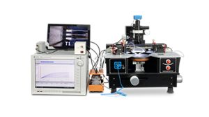
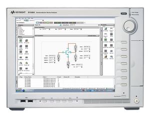
How to Evaluate IV Characteristics of LEDs
Characterizing current and voltage (IV) for energy-efficient LEDs requires the ability to generate and measure them simultaneously. Learn how to evaluate the IV characteristics of two- and three-terminal devices with a source / measure unit.
Learn More