


-
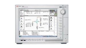
Parameter Analyzers
All-in-one systems for device characterization

-
Current-Voltage Analyzers
IV measurement systems for device characterization

-
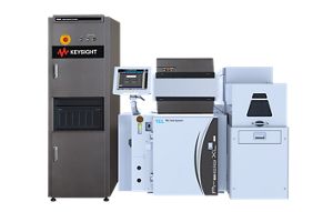
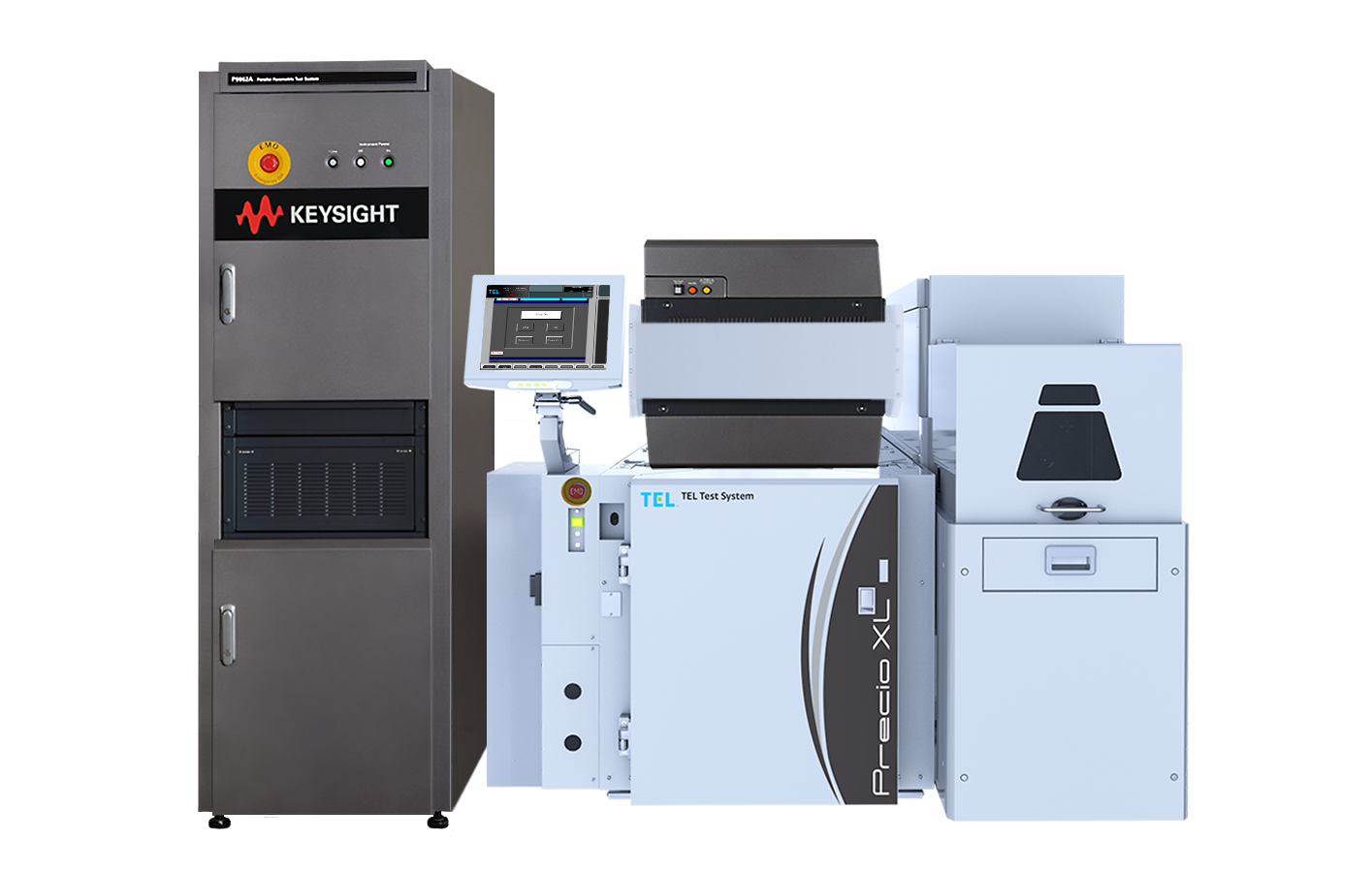
Parametric Test Solutions
Wafer-level test systems for parametric validation
-
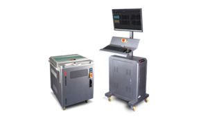
Electrical Structural Tester
Non-destructive electrical structural testing for wire bonds
-
Power Device Analyzer / Curve Tracer
High-power testing for Si, SiC, and GaN devices

-
Femto / Picoammeters and Electrometers
Instruments for measuring ultra-low current and high resistance

-
Universal Signal Processing Architecture
Real-time prototyping platform for silicon development

-
Low-Leakage Switch Matrix
High-isolation switching for ultra-low current routing


Parameter Analyzers
Keysight parameter analyzers provide comprehensive semiconductor device characterization in a single, integrated platform. Combining precision current-voltage (IV) and capacitance-voltage (CV) testing, pulsed measurements, and reliability testing, these modular systems support a wide range of devices from advanced materials to high-power components. With industry-leading measurement accuracy, flexible configuration options, and intuitive software control, Keysight parameter analyzers help accelerate device research, development, and qualification. Need help selecting? Check out the resources below.

Current-Voltage Analyzers
Keysight current-voltage analyzers deliver accurate, low-noise sourcing and measurement capabilities essential for semiconductor device characterization and material research. Designed to handle a broad range of current and voltage levels—from femtoamp currents to high-voltage sweeps—these analyzers provide precise, repeatable measurements across diverse applications. With flexible multi-channel configurations and intuitive software control, Keysight IV analyzers help accelerate device development, reliability testing, and process optimization. Need help selecting? Check out the resources below.

Parametric Test Solutions
Keysight parametric test solutions combine high-performance measurement instruments with flexible automation to accelerate semiconductor device evaluation from early development to high-volume production. Offering precise current-voltage (IV), capacitance-voltage (CV), and reliability testing, these scalable systems help optimize device performance, monitor process variability, and ensure long-term reliability. Designed for seamless integration with wafer probers and production environments, Keysight parametric solutions deliver the accuracy, speed, and efficiency needed for today’s advanced semiconductor technologies. Need help selecting? Check out the resources below.

Electrical Structural Tester
Keysight electrical structural testers are designed for semiconductor assembly and test applications requiring high-sensitivity detection of wire bond structural defects in post-mold IC packages. Leveraging nanoVTEP capacitive sensing and Part Average Testing (PAT), the system measures electrical coupling between pins to identify subtle deviations from known-good baselines without requiring functional power-up, using low-level electrical stimuli for measurement. Engineered for high-throughput manufacturing, it supports scalable multi-site configurations and parallel testing for consistent, high-coverage screening. With flexible architecture and seamless integration into production flows, it enables improved yield, reduced test escapes, and enhanced long-term reliability. Need help selecting? Check out the resources below.

Power Device Analyzer / Curve Tracer
Keysight power device analyzers / curve tracers are purpose-built solutions for evaluating and characterizing high-voltage, high-current semiconductor devices. Combining accurate sourcing, fast measurement, and comprehensive analysis, these systems support critical tests for power transistors, diodes, IGBTs, and wide bandgap devices such as SiC and GaN. With scalable voltage and current ranges, integrated safety features, and intuitive software, Keysight solutions help accelerate development, improve device reliability, and streamline production testing. Need help selecting? Check out the resources below.

Femto / Picoammeters and Electrometers
Keysight femto / picoammeters and electrometers deliver industry-leading sensitivity for measuring extremely low currents, high resistances, and low voltages in advanced materials and semiconductor devices. With measurement capabilities down to 0.01 fA and built-in graphical analysis, these instruments provide accurate, stable, and noise-resistant performance for demanding applications such as leakage current testing, insulation resistance, and ultra-low current characterization. Designed for both bench and system integration, Keysight’s precision electrometers help accelerate research, device development, and quality assurance. Need help selecting? Check out the resources below.

Universal Signal Processing Architecture
Keysight Universal Signal Processing Architecture (USPA) offers a high-performance, modular, fully programmable real-time environment for ultrafast application-specific prototyping and validation. Built around industry-leading ADC3 and DAC3 data converters and FPGA-based digital signal processing, the USPA platform empowers engineers to rapidly iterate and verify designs—reducing risk, development time, and cost. It supports applications spanning SoC/ASIC prototyping, 6G, optical communications, radar, and advanced physics research. Need help selecting? Check out the resources below.

Low-Leakage Switch Matrix
Keysight low-leakage switch matrices are designed for automated semiconductor testing that demands ultra-low current measurement and high isolation performance. Engineered to maintain signal integrity at femtoamp levels, these switch matrices enable seamless switching across multiple devices or test nodes without compromising measurement accuracy. With flexible configurations, compact form factors, and easy integration with Keysight analyzers, they are ideal for parametric testing, reliability studies, and wafer-level characterization. Need help selecting? Check out the resources below.

Explore High-Voltage Double-Pulse Testing
Validating next-generation power devices requires tools that deliver fast switching, precise timing, and robust safety under extreme conditions. The Keysight power device analyzer / curve tracer is purpose-built for dynamic characterization of SiC and GaN transistors, enabling accurate measurement of switching loss, dynamic on-resistance, and parasitic effects. With fully integrated control, built-in protection features, and high-voltage capabilities, it helps engineers replicate real-world stress conditions and accelerate power converter development, safely and reliably.
Find Compatible Software and Accessories for Your Semiconductor Test Solution
Choose from a wide variety of test, control, and application-specific software or accessories like low-leakage cabling, triaxial connectors, shielded switch extenders, wafer probe interfaces, and more.
Explore Semiconductor Use Cases
Semiconductor solutions support a wide-range of applications across various industries, discover them all.
Semiconductor
Characterizing WBG semiconductors with double-pulse test.


Semiconductor
Characterizing WBG semiconductor power modules using true pulse-isolated probe technology.

Semiconductor
Characterizing low-power ICs with a source measure unit.


Semiconductor
Evaluating IV LED characteristics using a source / measure unit.


Semiconductor
Eliminating error-inducing elements during resistance measurements.


Services and support
Innovate at speed with curated support plans and prioritized response and turn-around times.
Get predictable, lease-based subscriptions and full lifecycle management solutions—so you reach your business goals faster.
Experience elevated service as a KeysightCare subscriber to get committed technical response and more.
Ensure your test system performs to specification and meets local and global standards.
Make measurements quickly with in-house, instructor-led training, and eLearning.
Download Keysight software or update your software to the newest version.
Frequently Asked Questions
Semiconductors are materials with electrical conductivity between conductors and insulators, enabling controlled current flow in electronic devices.
- Common materials: silicon (Si), silicon carbide (SiC), gallium nitride (GaN)
- Function through doping to create p-type and n-type regions
- Form the basis of devices such as:
- Transistors (switching and amplification)
- Diodes (rectification)
- Integrated circuits (ICs)
- Enable key operations:
- Signal processing (analog and digital)
- Power conversion and regulation
- High-frequency communication (RF)
Their behavior is characterized using I-V, C-V, RF, and reliability measurements, which define performance in modern electronic systems.
Semiconductors are developed through a multi-stage process involving design, fabrication, packaging, and testing to ensure functionality and reliability.
-
Design phase:
- Circuit design (analog, digital, mixed-signal)
- Simulation and verification using EDA tools
-
Wafer fabrication:
- Photolithography, doping, etching, deposition
- Formation of transistors and interconnects on silicon wafers
-
Wafer-level testing:
- Electrical probing using I-V and C-V measurements
-
Packaging and assembly:
- Die separation, bonding, encapsulation
-
Final test and validation:
- Functional, parametric, and RF testing
- Reliability testing (stress, lifetime, thermal)
Organizations such as Keysight Technologies support these stages with measurement solutions spanning R&D through high-volume manufacturing.
Semiconductor performance is defined by electrical, physical, and reliability parameters measured across operating conditions.
-
Electrical characteristics (I-V):
- Threshold voltage, leakage current, on/off ratio
-
Capacitance characteristics (C-V):
- Doping profiles, oxide thickness, junction behavior
-
RF performance:
- Gain, noise figure, S-parameters, linearity
-
Power and switching behavior:
- Efficiency, switching speed, thermal performance
-
Reliability metrics:
- Lifetime, breakdown voltage, electromigration, stress tolerance
-
Process variation and yield:
- Wafer uniformity, device matching
Accurate characterization requires high-precision instrumentation, such as those provided by Keysight Technologies, across R&D and manufacturing environments.
Semiconductor test and measurement solutions are required for a wide range of devices, each with distinct electrical, thermal, and reliability challenges. Common device categories include:
- Discrete devices such as MOSFETs, IGBTs, diodes, and rectifiers used in power conversion
- Integrated circuits (ICs), including analog, digital, mixed-signal, and system-on-chip (SoC) devices
- Sensors, such as temperature, pressure, and optical sensors, which require precision and low-noise testing
- Wide bandgap semiconductors, including silicon carbide (SiC) and gallium nitride (GaN), used in high-voltage, high-frequency, and high-temperature applications
These devices require accurate characterization of current-voltage behavior, capacitance, leakage, switching dynamics, and reliability across operating conditions. Companies such as Keysight Technologies provide test platforms designed to support this full device spectrum from research through manufacturing.
Many semiconductor devices, particularly those used in low-power, precision, or next-generation applications, operate at extremely small current levels, sometimes in the femtoampere (fA) or picoampere (pA) range. At such scales, even trace amounts of leakage current or stray electrical interference from the test system itself can distort results, leading to inaccurate characterization. Low-leakage switch matrices are designed to minimize unwanted currents that could mask the true behavior of the device under test, while high-isolation measurement paths prevent crosstalk or noise coupling between signals. These features are especially important for characterizing sensitive devices like sensors, for testing advanced wide bandgap materials (SiC, GaN), or for conducting long-term reliability and stress tests where stable, repeatable measurements are essential. Without low-leakage and high-isolation performance, engineers risk drawing incorrect conclusions about device properties, potentially impacting design quality, safety, and compliance with application standards.
Characterizing semiconductor devices typically involves a range of complementary measurement techniques, each targeting specific electrical or physical parameters. Current-voltage (I-V) measurements form the foundation, providing insights into conduction, threshold voltages, leakage behavior, and breakdown characteristics across a wide voltage range. Capacitance-voltage (C-V) measurements are equally important, offering data on doping concentration profiles, oxide quality, and junction properties. Pulsed measurements are often employed for high-power or heat-sensitive devices, as they deliver short bursts of energy to prevent device degradation while still capturing dynamic behavior.
Reliability stress testing techniques, such as high-temperature operating life (HTOL), thermal cycling, and bias temperature instability (BTI) assessments, are used to simulate long-term operation and identify potential performance degradation mechanisms. In some cases, advanced methods like transient response analysis, time-dependent dielectric breakdown (TDDB), or radio-frequency (RF) characterization are also required, depending on the target application. Together, these techniques provide a comprehensive understanding of a semiconductor’s performance, robustness, and suitability for deployment.
Automation is a cornerstone of modern semiconductor testing, particularly in high-volume manufacturing environments or research laboratories handling complex multi-device characterization. By leveraging automated probe stations, robotic handlers, and software-driven test sequencing, organizations can significantly increase throughput, reduce operator error, and ensure consistent measurement repeatability across large data sets.
Automation also supports advanced capabilities such as unattended wafer probing, where hundreds or thousands of devices can be tested overnight, as well as automated batch testing for packaged devices. In reliability testing, automation enables continuous long-term stress monitoring without human intervention, ensuring early detection of performance drifts. Furthermore, automated systems facilitate data integration and analysis, allowing engineers to quickly identify trends, improve device models, and accelerate product development cycles. In short, automation not only enhances efficiency and productivity but also ensures quality control and compliance with rigorous industry standards at scale.
The semiconductor industry is characterized by rapid innovation, driven by new materials, advanced device architectures, and emerging application requirements. To remain effective, test systems must be both flexible and scalable. Modular platforms allow engineers to expand switching capacity, add new measurement modules, or integrate emerging test methodologies without requiring complete system replacement.
For instance, as wide bandgap semiconductors such as silicon carbide (SiC) and gallium nitride (GaN) become more prevalent in electric vehicles and renewable energy systems, test systems must incorporate capabilities for handling higher voltages, faster switching, and more demanding thermal conditions. Likewise, for next-generation communication and computing devices, high-speed transient analysis and radio-frequency (RF) testing are increasingly essential.
Adaptability also extends to software. Modern test systems must support evolving standards, data formats, and automation frameworks to ensure smooth integration into development workflows. By maintaining scalability and upgradeability, semiconductor test systems safeguard investment value while keeping pace with the continuous evolution of devices and applications.
Selecting semiconductor test solutions involves matching measurement capabilities to device type, operating conditions, and test requirements.
- Device category:
- Analog, digital, power, or RF devices require different setups
- Measurement needs:
- I-V (DC parametric testing)
- C-V (capacitance and doping analysis)
- RF (high-frequency characterization)
- Reliability (stress and lifetime testing)
- Voltage/current range:
- From low-power ICs to high-voltage SiC/GaN devices
- Accuracy and resolution:
- Critical for advanced nodes and precision devices
- Test environment:
- R&D characterization vs. high-volume manufacturing (ATE)
A structured approach ensures comprehensive validation, and organizations such as Keysight Technologies provide scalable solutions aligned with industry-standard measurement methodologies.