Choose a country or area to see content specific to your location
What are you looking for?
-
-
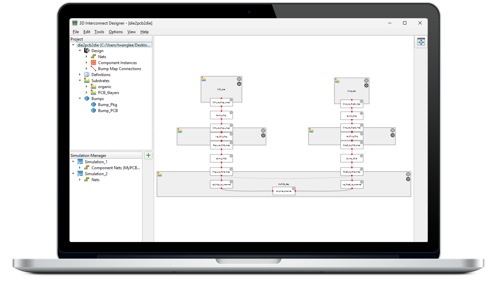
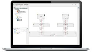
Accelerate Advanced Package & 3DIC DesignsAccelerate Advanced Package & 3DIC Designs
Design, model, and validate complex 3D interconnect architectures with a powerful standalone design environment.

-
Scale AI Compute. Simplify Validation.Scale AI Compute. Simplify Validation.
Automate transmitter and receiver validation across next-generation I/O, memory, and fabric interfaces.
-
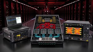
End-to-End Validation for AI Data CenterEnd-to-End Validation for AI Data Center
Strengthen 1.6T network reliability for AI-scale workloads from transceivers to interconnects.

-
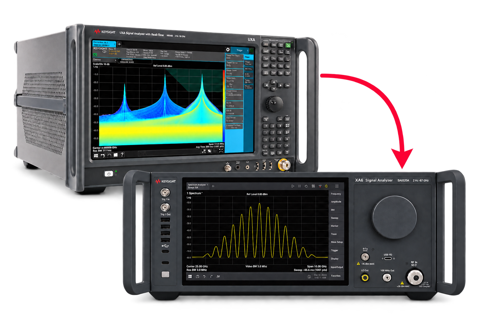
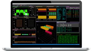
Take On Complex MIMO SignalsTake On Complex MIMO Signals
Pair Keysight VSA software with the new XA5 signal analyzer for advanced visualization, demodulation, and analysis — start your 30-day trial today.
-
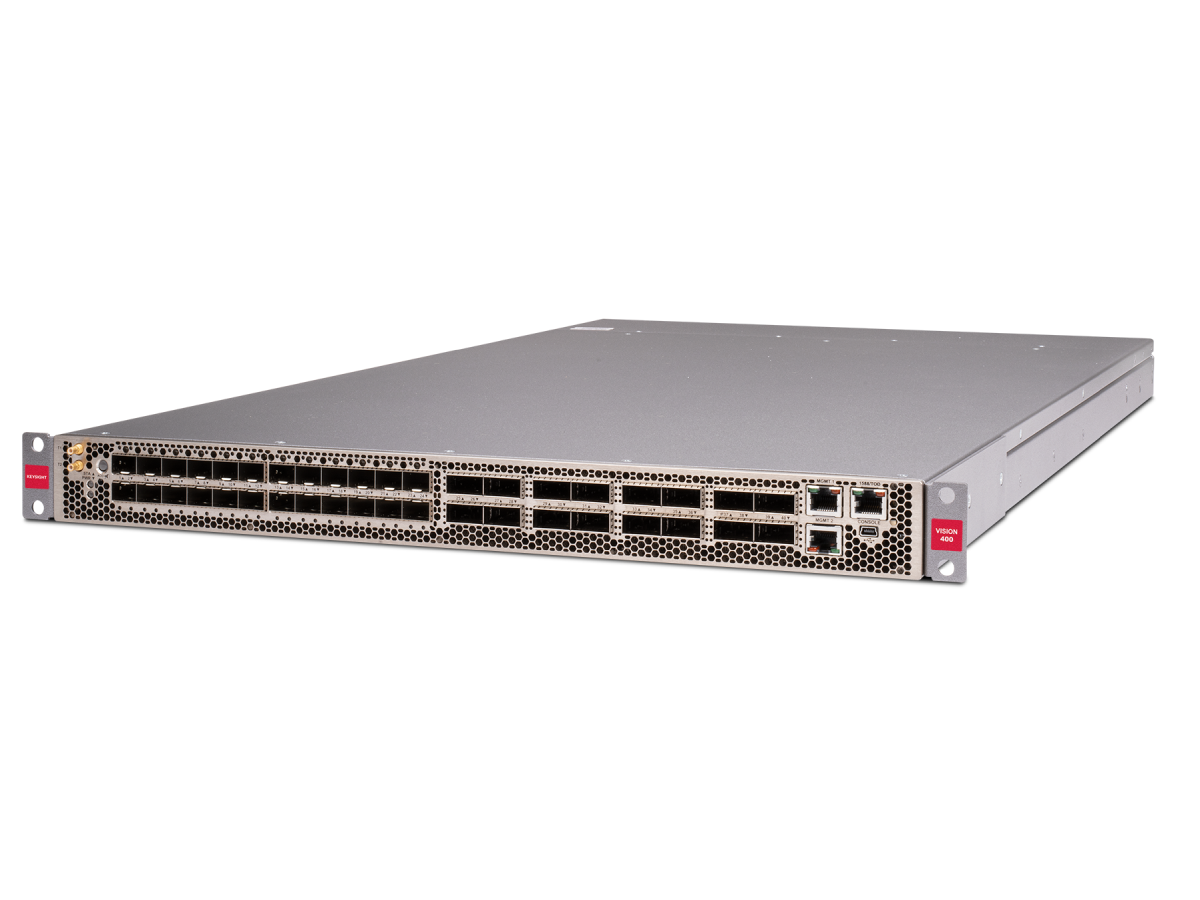
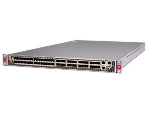
Introducing AI-Enhanced Packet BrokersIntroducing AI-Enhanced Packet Brokers
With extra memory and storage, these enhanced NPBs run Keysight's AI security and performance monitoring software and AI stack.
-
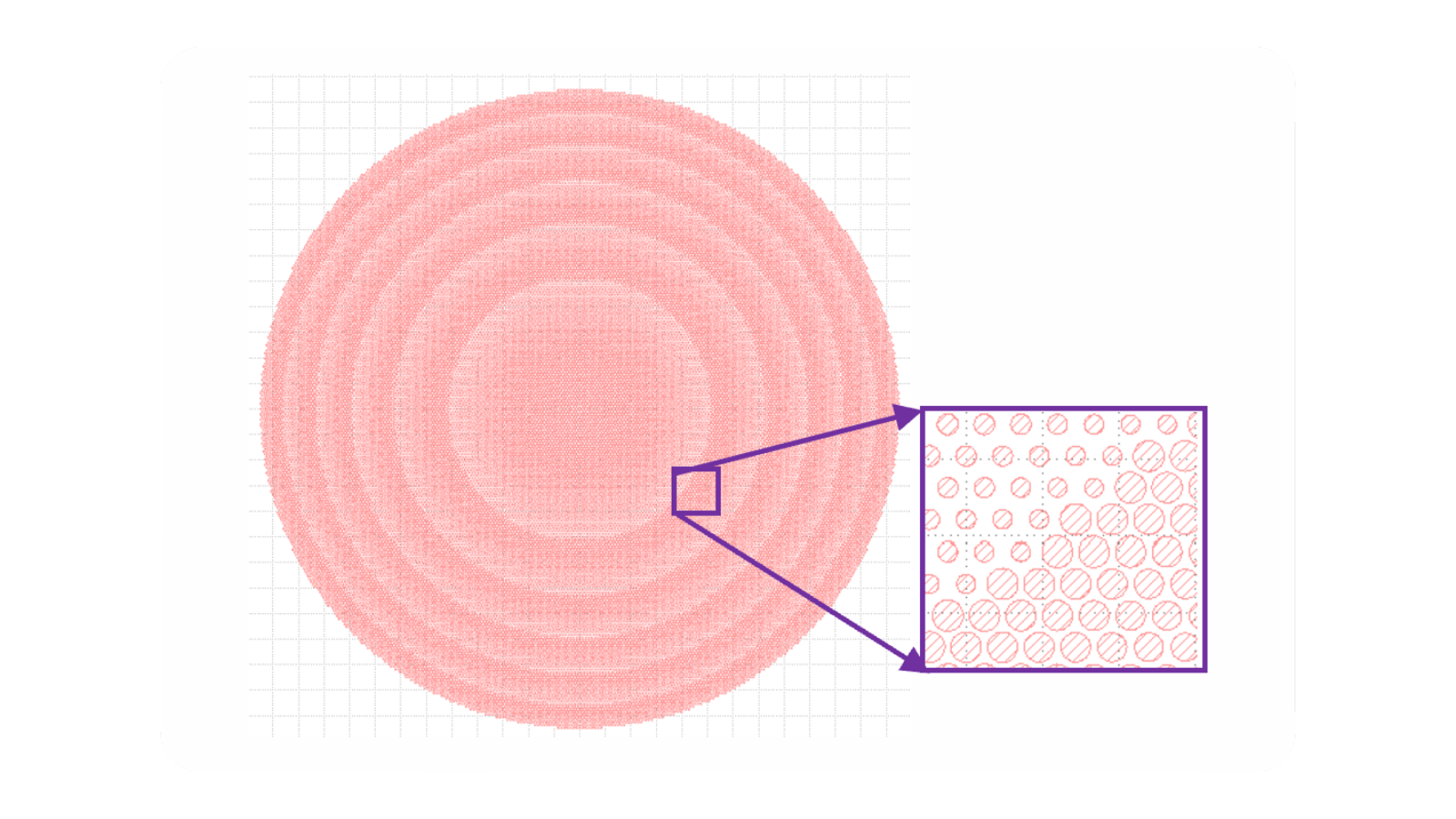
Accelerate Semiconductor InnovationAccelerate Semiconductor Innovation
Explore end-to-end workflows spanning IC design, validation, wafer test, and photonics.

-
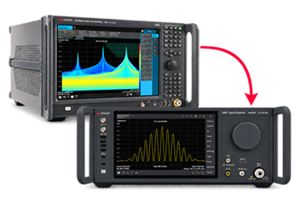
Trade In Before You Buy NewTrade In Before You Buy New
Save up to 50% on our latest instruments with eligible Keysight or competitor trade-ins.
-
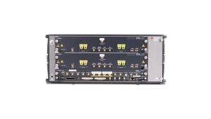
448 Gb/s Waveform Generation448 Gb/s Waveform Generation
Achieve 200+ Gbaud multi-level modulated signals with high-speed AWGs for digital and optical standards.
-
The Right Connection Makes the MeasurementThe Right Connection Makes the Measurement
Maximize accuracy and performance with precision accessories engineered for Keysight instruments.

Trade In Before You Buy NewTrade In Before You Buy NewSave up to 50% on our latest instruments with eligible Keysight or competitor trade-ins.
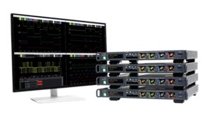
Scale to Hundreds of Channels. Keep Measurements in Sync.Scale to Hundreds of Channels. Keep Measurements in Sync.Four channels per 1U of rack space, up to 1 GHz bandwidth, and multi-oscilloscope synchronization.
-
-
Purpose-built solutions engineered for the design and test challenges unique to your industry.
FeaturedUse Cases mapped to every stage of your product lifecycle, from design through operations.
Nokia + Keysight: AI Network Designs at ScaleSuccess Stories
Nokia + Keysight: AI Network Designs at Scale -
Authoritative application notes, data sheets, reference designs, and test procedures to accelerate design and validation decisions.
FeaturedHands‑on bootcamps that teach system design, test methods, and production workflows engineers can apply immediately.
AI TechnologyLearning Hub
AI TechnologyExplore methodologies, test strategies, and technical resources for designing, validating, and scaling AI systems and networks.
- Buy
-
Quick access to support related self-help tasks.
Additional content to support your product needs.
Do more with Keysight ServicesDo more with Keysight ServicesExplore services to accelerate every step of your innovation journey.