Choose a country or area to see content specific to your location
What are you looking for?
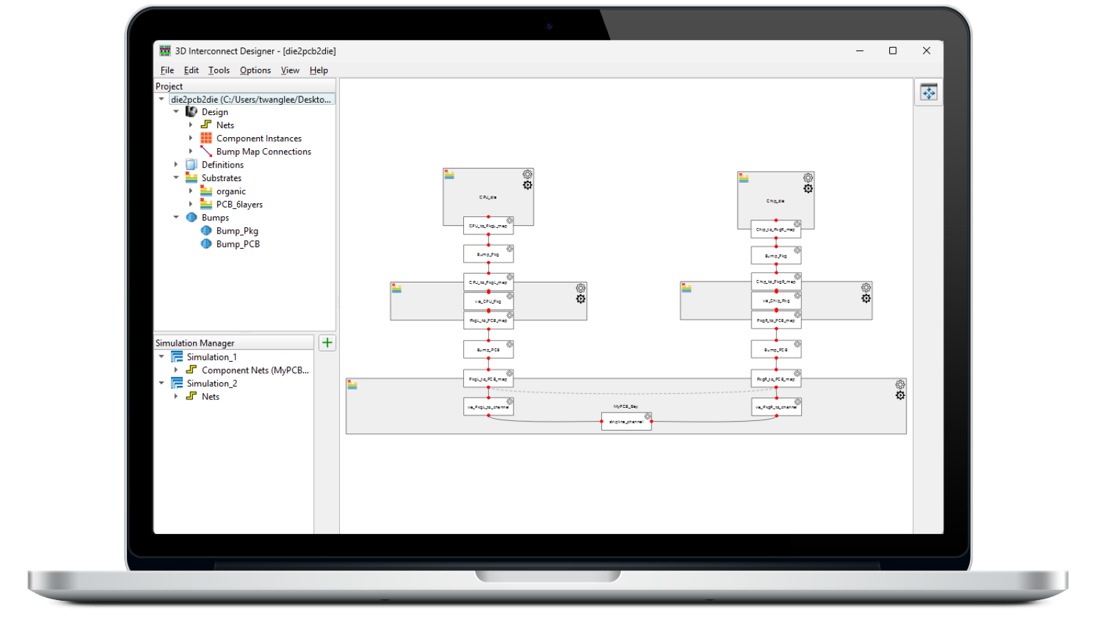
Design, model, and validate complex 3D interconnect architectures with a powerful standalone design environment.
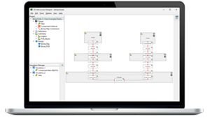
Automate transmitter and receiver validation across next-generation I/O, memory, and fabric interfaces.
Strengthen 1.6T network reliability for AI-scale workloads from transceivers to interconnects.

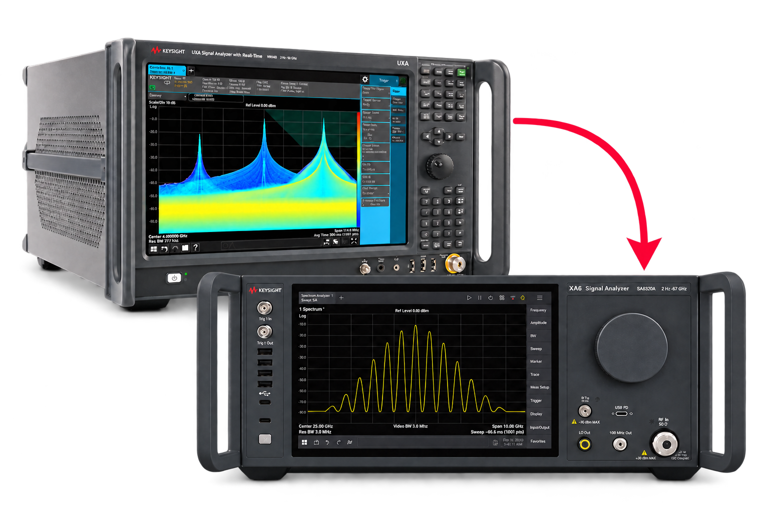
Pair Keysight VSA software with the new XA5 signal analyzer for advanced visualization, demodulation, and analysis — start your 30-day trial today.
With extra memory and storage, these enhanced NPBs run Keysight's AI security and performance monitoring software and AI stack.
Explore end-to-end workflows spanning IC design, validation, wafer test, and photonics.

Save up to 50% on our latest instruments with eligible Keysight or competitor trade-ins.
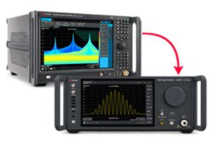
Achieve 200+ Gbaud multi-level modulated signals with high-speed AWGs for digital and optical standards.
Maximize accuracy and performance with precision accessories engineered for Keysight instruments.
Save up to 50% on our latest instruments with eligible Keysight or competitor trade-ins.
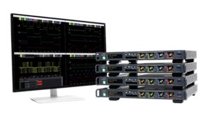
Four channels per 1U of rack space, up to 1 GHz bandwidth, and multi-oscilloscope synchronization.
Purpose-built solutions engineered for the design and test challenges unique to your industry.
Use Cases mapped to every stage of your product lifecycle, from design through operations.
Success Stories
Authoritative application notes, data sheets, reference designs, and test procedures to accelerate design and validation decisions.
Hands‑on bootcamps that teach system design, test methods, and production workflows engineers can apply immediately.
Learning Hub
Explore methodologies, test strategies, and technical resources for designing, validating, and scaling AI systems and networks.
Quick access to support related self-help tasks.
Additional content to support your product needs.
Explore services to accelerate every step of your innovation journey.
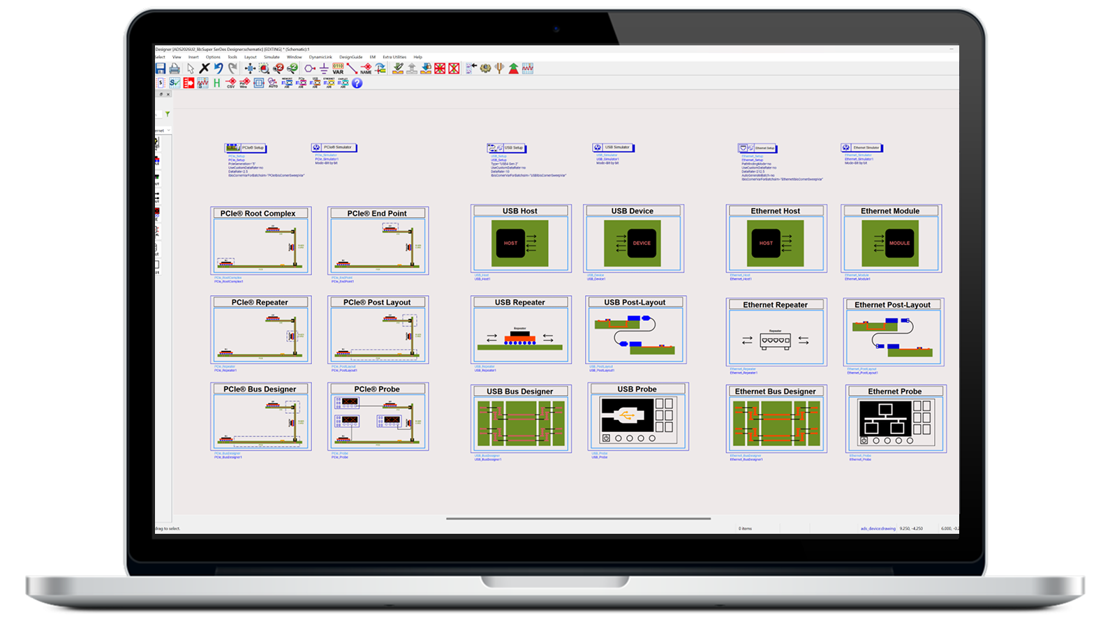
Streamlined SerDes system analysis with end-to-end design workflows in a single package.
A standards-driven, or standards-aware workflow is a key enabler for accelerating time-to-market, reducing late-stage design risks, and improving overall engineering productivity by increasing design confidence throughout the product development cycle. The SerDes Designer brings together the core strengths of the System Designer series, allowing USB, PCIe ®, and Ethernet Designer to be used within a single product solution. Maximize productivity with a smart design workflow, allowing a lean engineering team to handle multiple SerDes interfaces simultaneously with a single-license solution, offering a highly cost-effective path to high-performance designs and faster product-to-market.
ADS Software Bundles provide circuit and component designers with a choice of value-packed, preconfigured combinations of software modules built for specific design workflows. These combinations start with the powerful core ADS functionality for 3D physical layout and verification, data display, optimization, Python scripting automation and statistical analysis.
Webinars
Webinars
Bootcamps
White Papers
Case Studies
Discover the latest release designed to help engineers work faster, simulate more accurately, and accelerate product development.
SerDes Designer integrates System Designer for PCIe®, USB, and Ethernet into a single environment, enabling a unified and efficient workflow across multiple SerDes applications. It supports the latest standards and helps accelerate product development with AMI model generation and simulation-driven compliance testing.
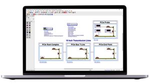
System Designer for PCIe® is a modern and smart PCIe design environment for modeling and simulating the latest PCIe Gen5 and Gen6 systems. It enables designers to perform complete PCIe system analysis and simulation-driven virtual compliance tests with a streamlined workflow.
W3651B
System Designer for PCIe® is a modern and smart PCIe design environment for modeling and simulating the latest PCIe Gen5 and Gen6 systems. It enables designers to perform complete PCIe system analysis and simulation-driven virtual compliance tests with a streamlined workflow.
The W3651B System Designer for PCIe® includes the following:
The System Designer for PCIe® automates the setup for multi-link, multi-lane, and multi-level (PAM4) PCIe systems using a smart design environment. The PCIe AMI modeler, which supports NRZ and PAM4 modulations, facilitates the quick implementation of PCIe systems. The integrated simulation-driven compliance test solution can reduce design costs by minimizing design iterations and shortening time-to-market.
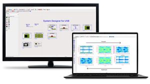
The System Designer for USB is a modern and smart USB design environment for modeling and simulating the latest USB4® Gen2, Gen3 and Gen4 systems. It enables designers to perform complete USB system analysis and simulation-driven virtual compliance tests with a streamlined workflow.
W3652B
The System Designer for USB is a modern and smart USB design environment for modeling and simulating the latest USB4® Gen2, Gen3 and Gen4 systems. It enables designers to perform complete USB system analysis and simulation-driven virtual compliance tests with a streamlined workflow.
The W3652B System Designer for USB includes:
The System Designer for USB streamlines the setup of complex USB system, including multi-link, multi-lane, and multi-level (PAM3) configuration, through a smart design environment. The USB AMI modeler, which supports both NRZ and PAM3 modulations, enables the rapid and efficient USB systems implementation. Additionally, the integrated simulation-driven compliance test solution helps reduce design costs by minimizing design iterations and shortening time-to-market.
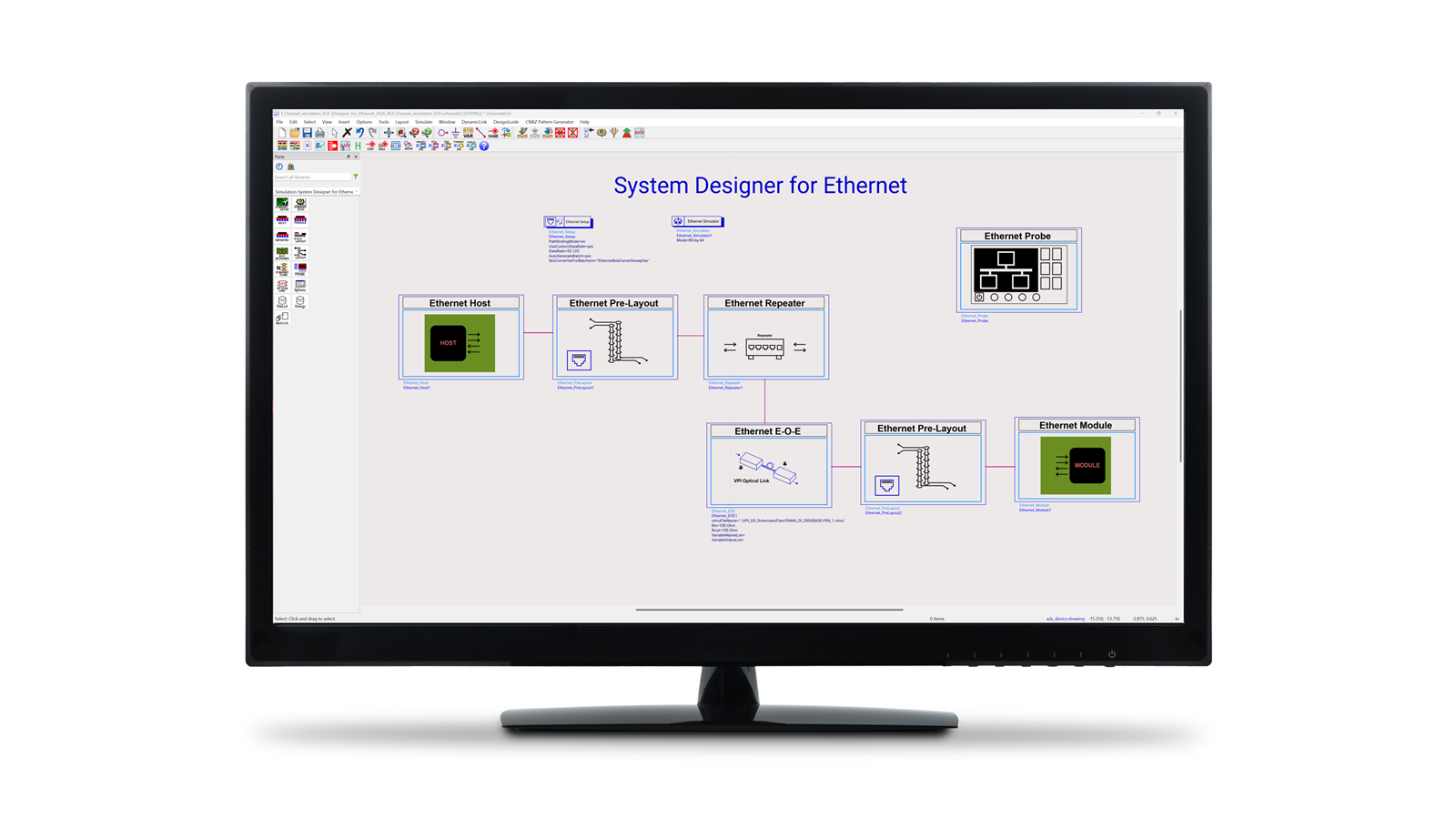
System Designer for Ethernet offers a unified and streamlined design workflow solution for analyzing the latest Ethernet standards, covering speeds from 100G to 1.6Tb/s. It helps designers accelerate product development and validation of next-generation Ethernet systems through a smart workflow and AMI model generation capability.
W3653B
System Designer for Ethernet offers a unified and streamlined design workflow solution for analyzing the latest Ethernet standards, covering speeds from 100G to 1.6Tb/s. It helps designers accelerate product development and validation of next-generation Ethernet systems through a smart workflow and AMI model generation capability.
The W3653B System Designer for Ethernet includes the following:
The System Designer for Ethernet automates the setup of multi-link, multi-lane, and multi-level (PAM4) Ethernet systems using a smart design environment. The Ethernet AMI modeler enables rapid implementation of Ethernet systems. The interface to COM (Channel Operating Margin) calculation helps reduce design costs by minimizing design iterations and shortening time-to-market.
High-speed digital design is a subset of electronic design that deals with the physical layer of digital circuits and communication systems operating at high data rates. It requires special attention to the effects of signal integrity, power integrity, electromagnetic interference, and thermal management. High-speed digital design can enable faster data transfer, lower power consumption, and higher performance in electronic systems.
Standards-driven design is an electronic design method that follows predefined specifications and protocols for communication, data exchange, and interoperability between different devices and systems. Standards-based design can facilitate compatibility, reliability, and scalability in electronic systems. Examples of standards-based design include USB, PCIe®, UCIe, and DDR.
Keysight EDA’s ADS SerDes design solution offers a comprehensive design and simulation platform that effectively streamlines the SerDes design workflow, empowering designers to overcome challenges, reduce time-to-market, and refine design iterations. It covers various SerDes standards, including PCIe®, USB, Ethernet, MIPI®, and more.
Universal Serial Bus (USB) is a standard for communication and power delivery between devices and hosts, such as computers, smartphones, cameras, and peripherals. USB supports various data rates, from 1.5 Mbps (USB 1.0) to 80 Gbps (USB4 Version 2.0). USB also supports different power delivery modes, from 2.5 W (USB 2.0) to 240 W (USB PD 3.1). USB4 Version 2.0 is the latest version of the standard and is backward compatible with USB 3.2, USB 2.0, and Thunderbolt 3.
Peripheral Component Interconnect Express (PCIe) is a standard for high-speed serial communication between devices and hosts, such as computers, graphics cards, network cards, and storage devices. PCIe supports various data rates, from 2.5 GT/s (PCIe 1.0) to 64 GT/s (PCIe 6.0). The PCI Special Interest Group (PCI-SIG®) defines specifications and compliance tests that guarantee the interoperability of PCIe systems. PCIe also supports different lane configurations, from x1 to x32, to increase bandwidth and performance.
Talk to our team to find the right solution for your design needs, get a personalized quote, or request a free trial.
What are you looking for?