Choose a country or area to see content specific to your location
What are you looking for?
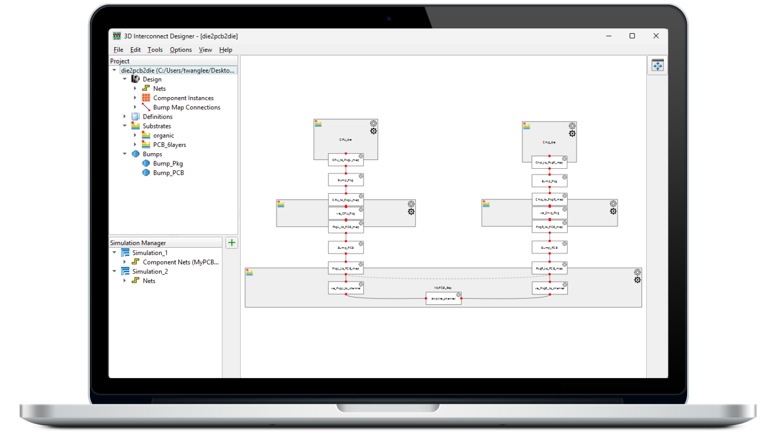
Design, model, and validate complex 3D interconnect architectures with a powerful standalone design environment.
Automate transmitter and receiver validation across next-generation I/O, memory, and fabric interfaces.
Strengthen 1.6T network reliability for AI-scale workloads from transceivers to interconnects.
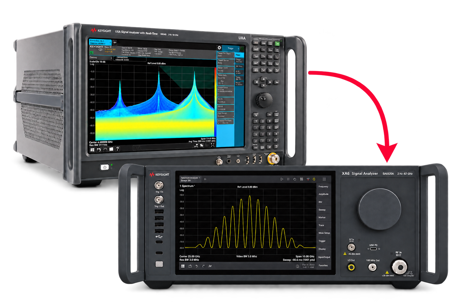
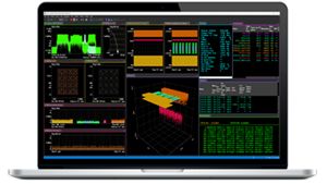
Pair Keysight VSA software with the new XA5 signal analyzer for advanced visualization, demodulation, and analysis — start your 30-day trial today.
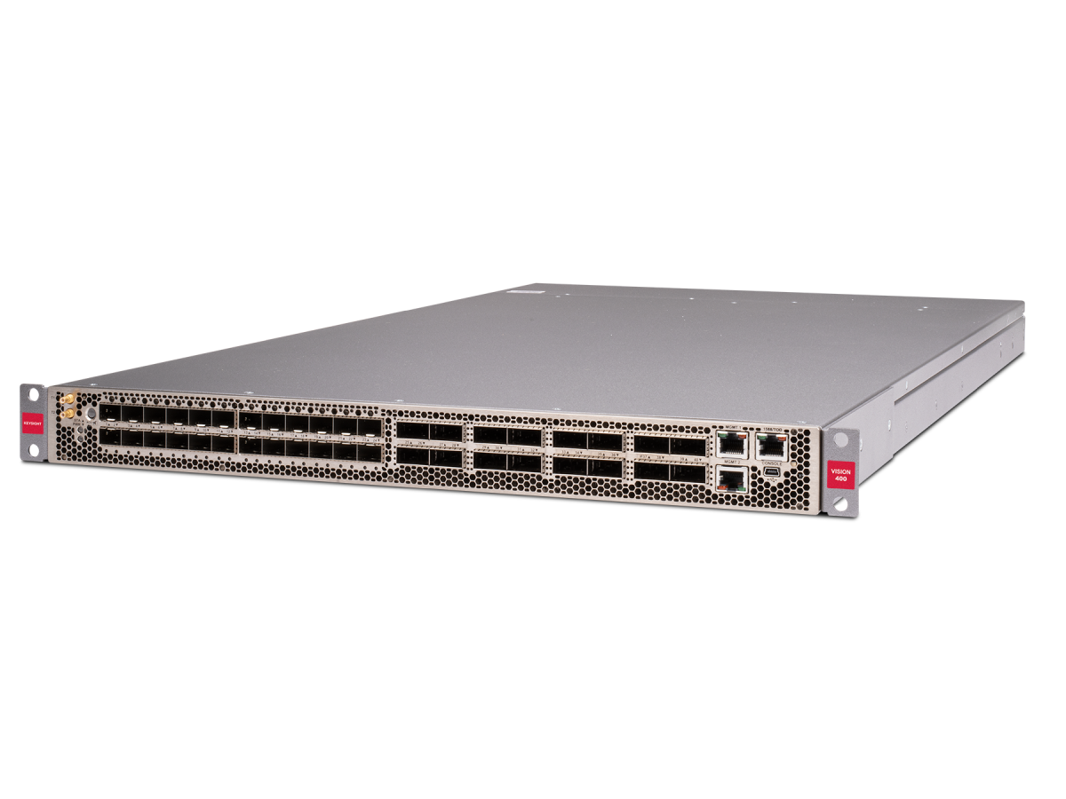
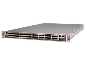
With extra memory and storage, these enhanced NPBs run Keysight's AI security and performance monitoring software and AI stack.
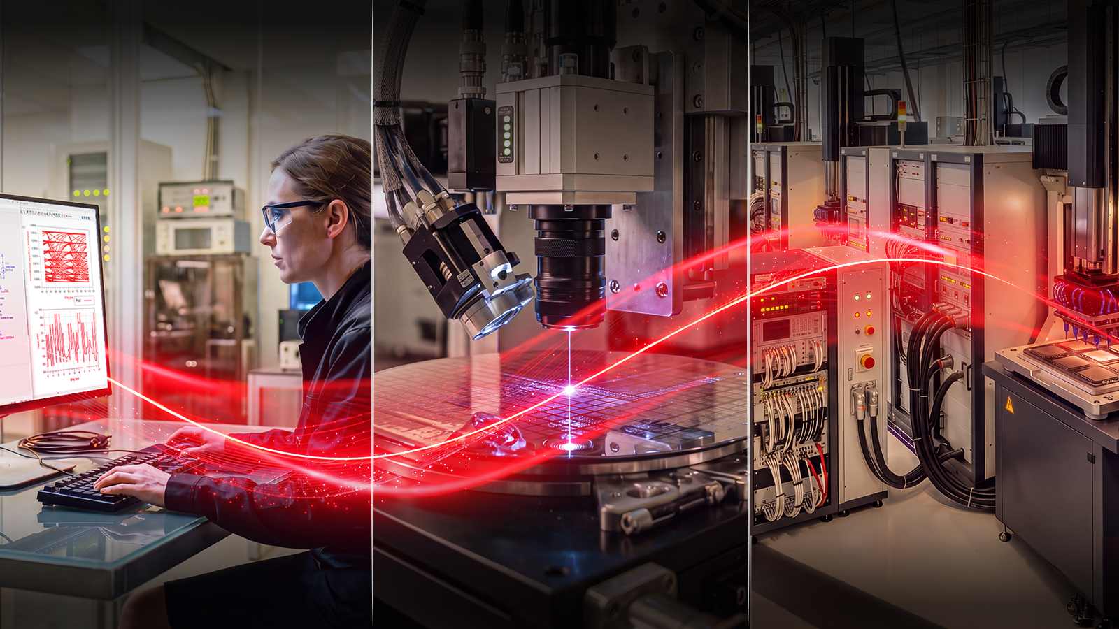
Explore end-to-end workflows spanning IC design, validation, wafer test, and photonics.
Save up to 50% on our latest instruments with eligible Keysight or competitor trade-ins.
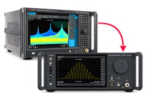
Achieve 200+ Gbaud multi-level modulated signals with high-speed AWGs for digital and optical standards.
Maximize accuracy and performance with precision accessories engineered for Keysight instruments.
Save up to 50% on our latest instruments with eligible Keysight or competitor trade-ins.
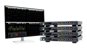
Four channels per 1U of rack space, up to 1 GHz bandwidth, and multi-oscilloscope synchronization.
Purpose-built solutions engineered for the design and test challenges unique to your industry.
Use Cases mapped to every stage of your product lifecycle, from design through operations.
Success Stories
Authoritative application notes, data sheets, reference designs, and test procedures to accelerate design and validation decisions.
Hands‑on bootcamps that teach system design, test methods, and production workflows engineers can apply immediately.
Learning Hub
Explore methodologies, test strategies, and technical resources for designing, validating, and scaling AI systems and networks.
Quick access to support related self-help tasks.
Additional content to support your product needs.
Explore services to accelerate every step of your innovation journey.
Get a deeper, closer look at low frequency noise with the A-LFNA integrated with WaferPro Express, featuring data analysis, wafer prober control and test suite automation.
Turn critical noise data into better models and more reliable designs.
Low-frequency flicker noise and random telegraph noise (RTN) increasingly impact advanced analog, RF, and power semiconductor technologies. Keysight A-LFNA helps engineers gain deeper insight into device behavior through highly sensitive and repeatable noise characterization, enabling more accurate model development and technology qualification.
Integrated with WaferPro, A-LFNA extends automated characterization workflows beyond DC, CV, and RF measurements to include low-frequency noise analysis within a single platform. This unified approach improves measurement consistency, reduces manual effort, and accelerates the delivery of high-quality data for PDK development, model generation, and process qualification.
Advanced low-frequency noise analyzer’s integration with Device Modeling WaferPro enables turnkey noise measurements as well as the measurement of DC characteristics, capacitance, and RF S-parameters.
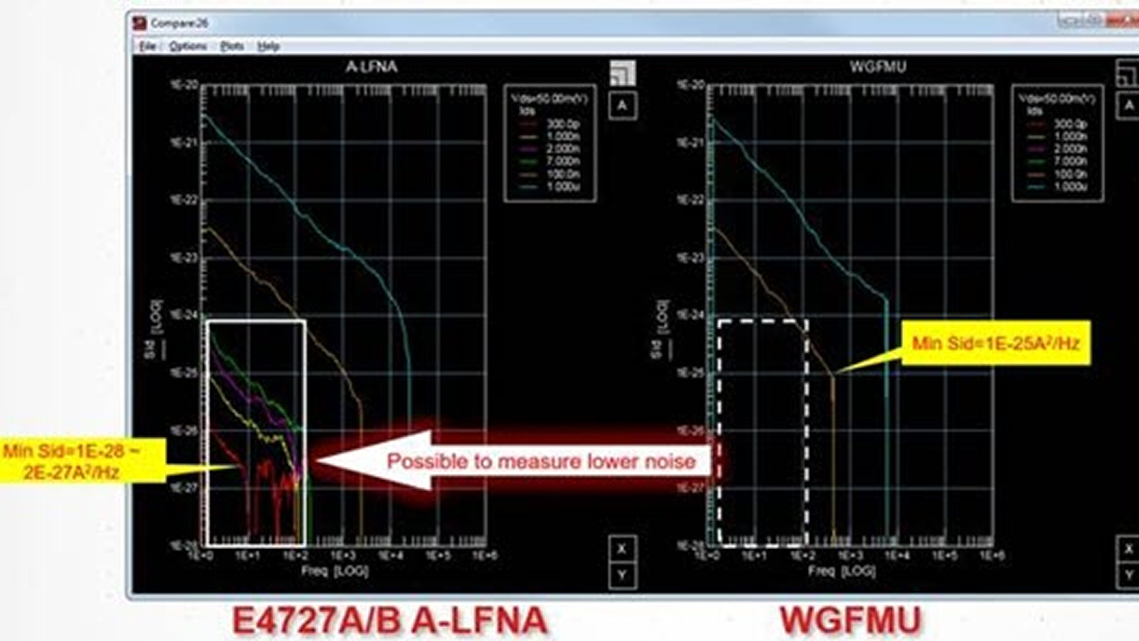
Extremely low device noise measurement such as transistor linear region noise by newly designed LNA.
State-of-the-art new LNA also allows noise measurement in very low bias current.
High-power device noise measurement even in a high current like 1A.
Improve measurement productivity by fast measurement speed even in the high accurate conditions with several averaging.
The software module measures DC characteristics, 1/f noise, and random telegraph noise and conducts data analysis.
Keysight’s close collaboration with FormFactor enables a complete integrated on-wafer solution with automated control of all major wafer probing systems.
The A-LFNA’s built-in measurement routines make DC and noise measurements turnkey. For example, to measure noise on an N-Type MOSFET, the system automatically chooses the source and load impedances that will best expose the intrinsic device noise. The engineer can accept these recommended settings or make changes, and a noise measurement is initiated. The A-LFNA then measures noise power spectral density (1/f noise) and noise in the time domain (RTN). The resulting data is plotted using a multiplot data display window. Various windows' tabs help facilitate common tasks such as evaluating the device's DC operating point and measuring the slope of the power spectral density curve. Noise data can also be analyzed and represented in device models using device modeling tools such as Device Modeling (MBP) and Device Modeling (IC-CAP). Circuit designers can use these device models to ensure highly accurate RF and analog low-noise circuit design.
W7801B (Device Modeling WaferPro WGFMU Measurement bundle) efficiently performs at a low cost and automated RTN measurement on the wafer using the B1500A Semiconductor Device Analyzer with the B1530A Waveform Generator/Fast Measurement Unit (WGFMU). It can improve the efficiency of RTN measurement and data analysis including wafer prober control.
Key features
The Keysight E4727B/W7802B is a turn-key solution to measure flicker (1/f) noise and RTN (Random Telegraph Noise) of a semiconductor's device. The Keysight W7801B is bundle software to control Keysight B1530A (WGFMU). These solutions can control semi-auto probe stations and get mass wafer mapping noise data automatically.
Webinars
Case Studies
Application Notes
Application Notes
The Keysight E4727B Advanced Low-Frequency Noise Analyzer is a turnkey solution for fast, accurate, and repeatable low-frequency noise measurements. It characterizes flicker (1/f) noise and random telegraph noise (RTN) in semiconductor devices, supporting advanced device modeling and reliability analysis.
The E4727B measures DC characteristics, 1/f noise, and random telegraph noise while providing integrated data analysis capabilities. It also supports automated wafer-level testing and can be combined with capacitance and RF measurements.
The analyzer provides industry-leading sensitivity for detecting extremely low noise levels across a wide range of device types. This helps engineers develop accurate device models and identify performance-limiting noise mechanisms earlier.
Yes. Integration with Keysight WaferPro Express enables automated wafer probing, wafer mapping, and test sequencing. Engineers can efficiently collect large volumes of low-frequency noise data across entire wafers.
The E4727B supports process design kit (PDK) development, IC noise specification, manufacturing process control, reliability studies, and semiconductor device modeling for low-noise electronic designs.
Talk to our team to find the right solution for your design needs, get a personalized quote, or request a free trial.
What are you looking for?