Choose a country or area to see content specific to your location
What are you looking for?
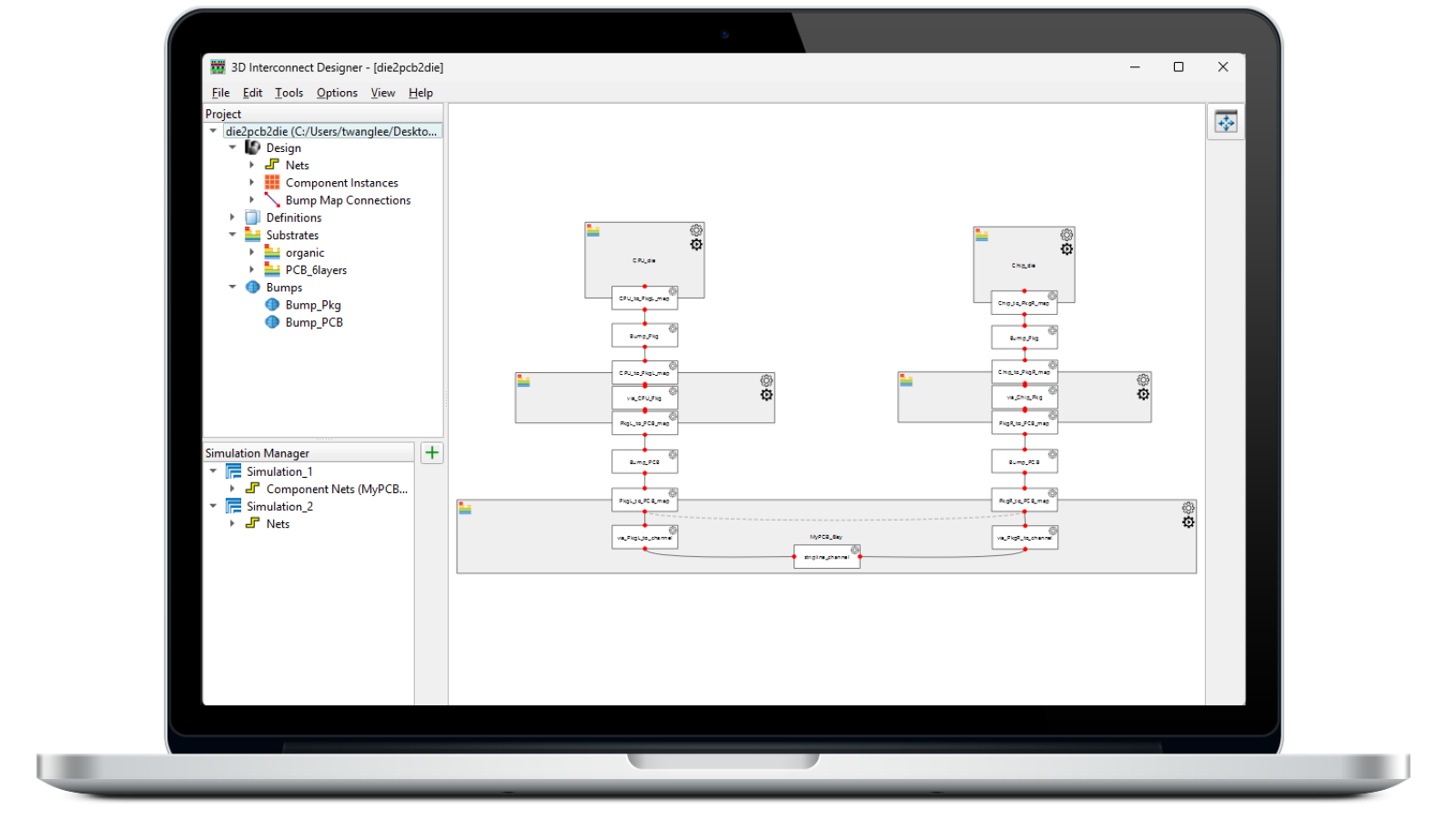
Design, model, and validate complex 3D interconnect architectures with a powerful standalone design environment.
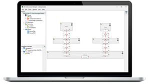
Automate transmitter and receiver validation across next-generation I/O, memory, and fabric interfaces.

Strengthen 1.6T network reliability for AI-scale workloads from transceivers to interconnects.

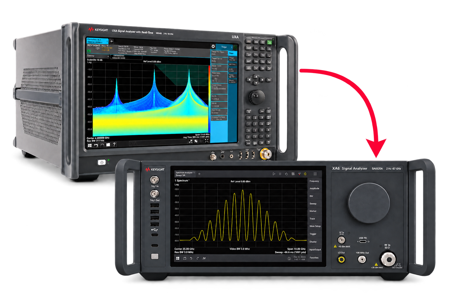
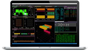
Pair Keysight VSA software with the new XA5 signal analyzer for advanced visualization, demodulation, and analysis — start your 30-day trial today.
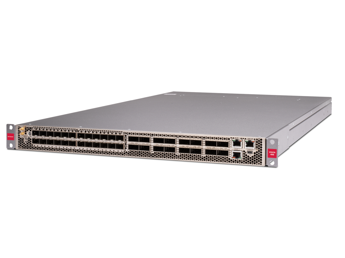
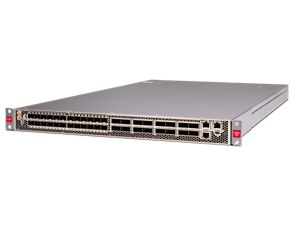
With extra memory and storage, these enhanced NPBs run Keysight's AI security and performance monitoring software and AI stack.
Explore end-to-end workflows spanning IC design, validation, wafer test, and photonics.

Save up to 50% on our latest instruments with eligible Keysight or competitor trade-ins.
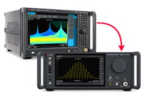
Achieve 200+ Gbaud multi-level modulated signals with high-speed AWGs for digital and optical standards.
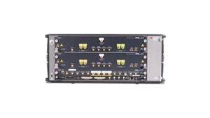
Maximize accuracy and performance with precision accessories engineered for Keysight instruments.
Save up to 50% on our latest instruments with eligible Keysight or competitor trade-ins.
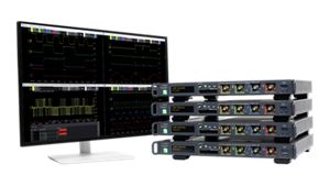
Four channels per 1U of rack space, up to 1 GHz bandwidth, and multi-oscilloscope synchronization.
Purpose-built solutions engineered for the design and test challenges unique to your industry.
Use Cases mapped to every stage of your product lifecycle, from design through operations.
Success Stories
Authoritative application notes, data sheets, reference designs, and test procedures to accelerate design and validation decisions.
Hands‑on bootcamps that teach system design, test methods, and production workflows engineers can apply immediately.
Learning Hub
Explore methodologies, test strategies, and technical resources for designing, validating, and scaling AI systems and networks.
Quick access to support related self-help tasks.
Additional content to support your product needs.
Explore services to accelerate every step of your innovation journey.
Analyze photonic crystal band structures before fabrication.
Optimize the band structure of photonic crystal geometries.
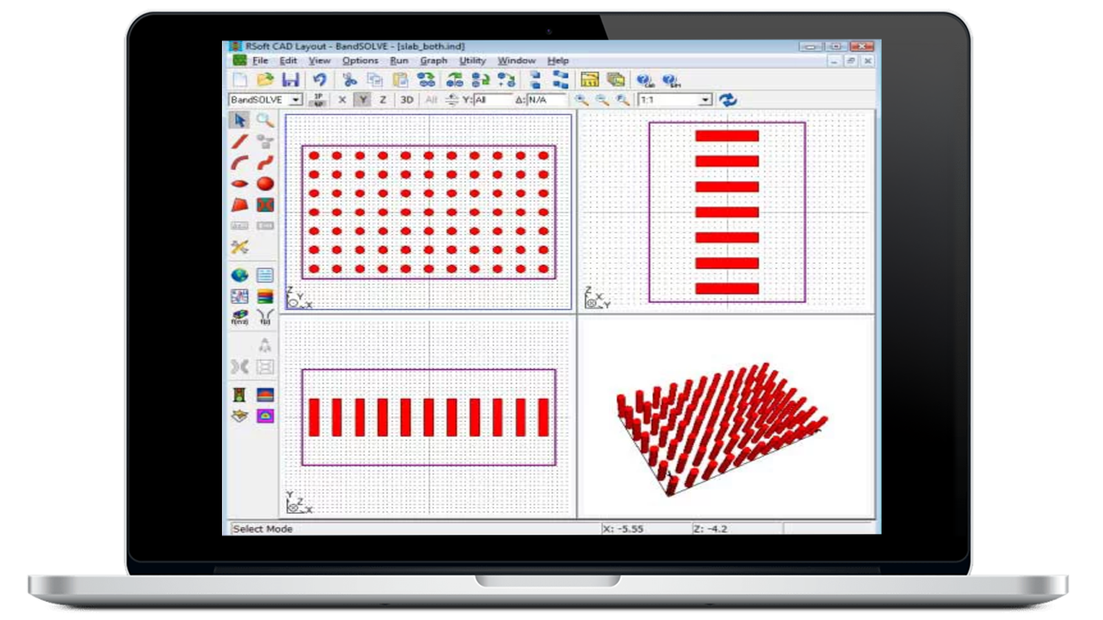
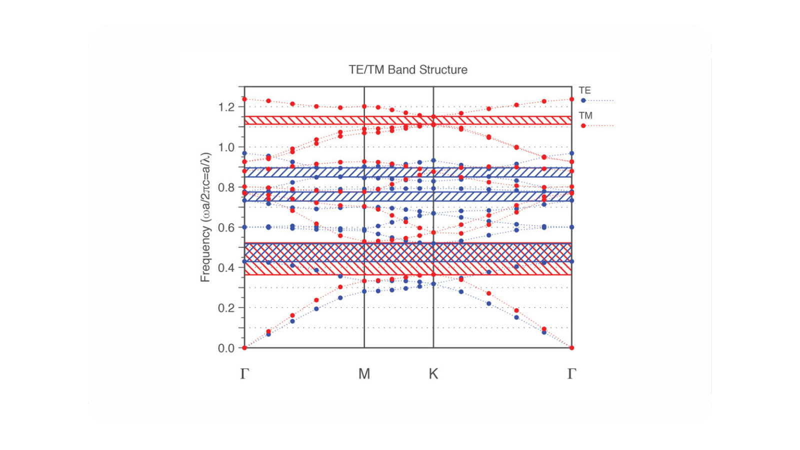
Automate and simplify modeling and calculation of photonic band structures for all photonic crystal devices with RSoft BandSOLVE. BandSOLVE’s simulation engine employs a plane wave expansion (PWE) design tool to perform band computations. It also provides a graphical display of electromagnetic fields and other quantities for further analysis.
With a built-in array layout utility and layout hierarchy, your team can conveniently create standard and custom photonic band gap (PBG) structures. BandSOLVE also optimizes the band structure of new photonic crystal geometries before fabricating a device, allowing you to determine the performance of existing components.
Determine frequency ranges in which light propagation is allowed or inhibited before fabricating the structure.
Examine Bloch modes, defect modes, and field distributions to understand how structural changes affect light propagation.
Evaluate alternative lattice, material, and defect configurations within a consistent simulation workflow.
Use band-structure results to select promising designs for more detailed electromagnetic analysis.
Analyze periodic optical structures and photonic crystal devices.
• Photonic crystal waveguides
• Photonic crystal fibers
• Photonic bandgap structures
• Resonant cavities
• Defect-mode devices
• Optical filters
• Periodic optical materials
• Integrated photonic components
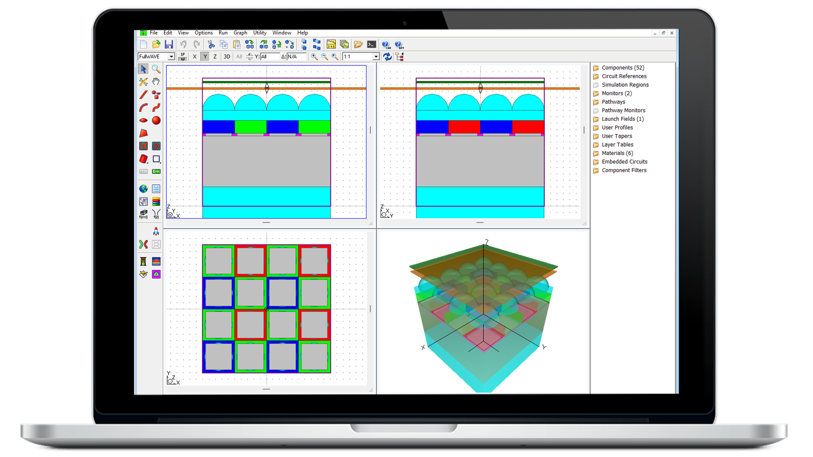
Use the RSoft FullWAVE FDTD simulation tool to study how light propagates in photonic structures, circuits, and nanophotonic devices.
Use RSoft FemSIM FEM design tool to calculate any number of transverse or cavity modes of an arbitrary structure on a non-uniform mesh.
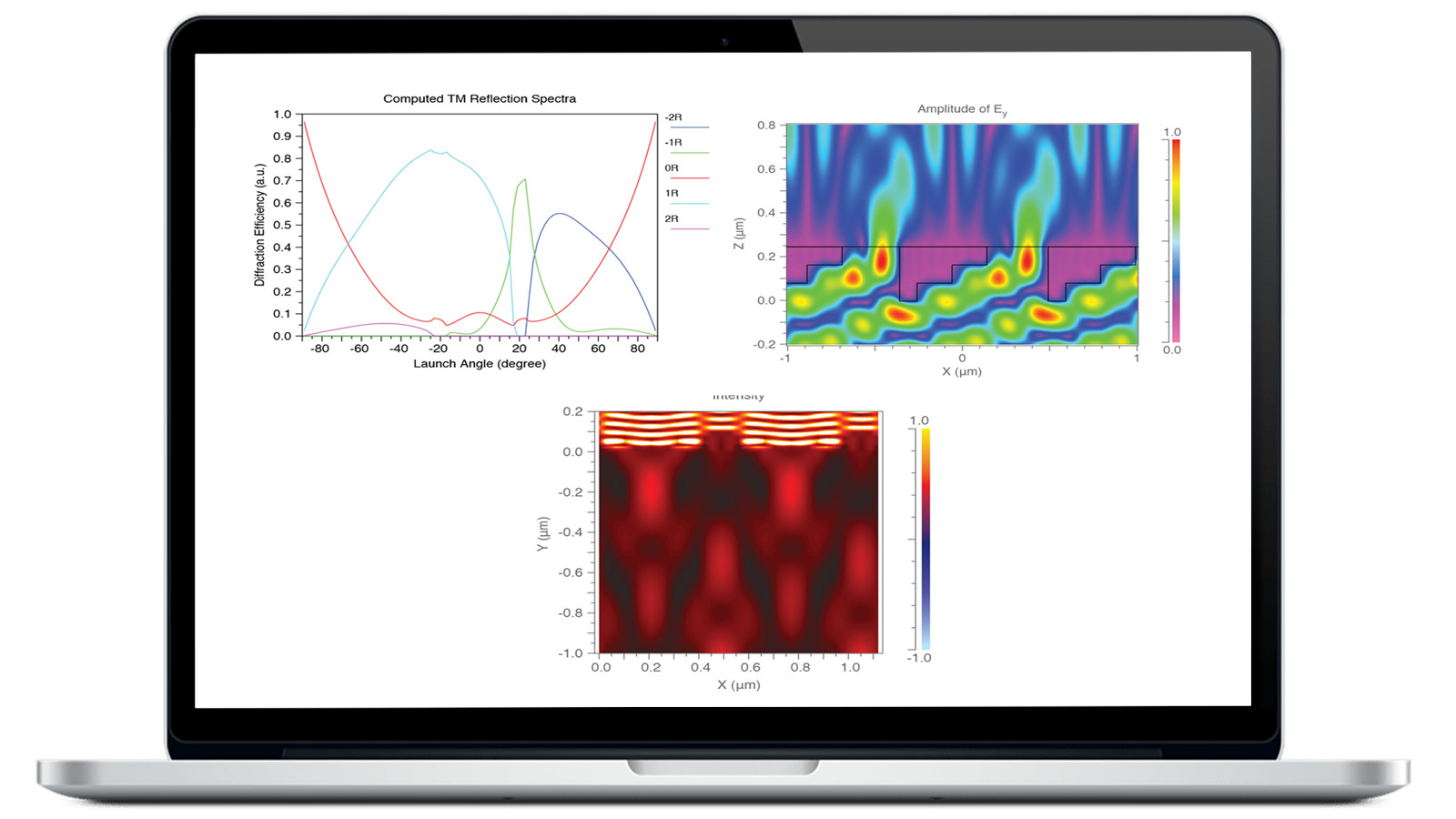
Use DiffractMOD RCWA design tool for diffractive optical structures, subwavelength periodic structures, photonic bandgap crystals, and more.
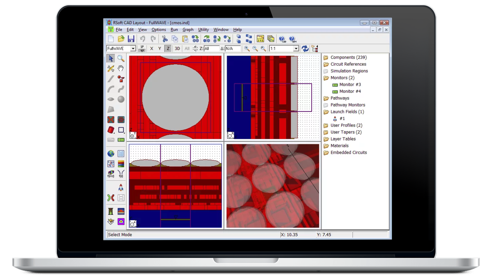
The RSoft CAD Environment is the core program of the RSoft photonic device tools. Design waveguide devices, optical circuits, and other photonic devices.
Learn how band diagrams are used to analyze photonic crystal structures and identify photonic band gaps before fabrication.
The plane wave expansion (PWE) method is a frequency-domain simulation technique used to calculate the band structure of periodic optical materials and photonic crystals. By solving for the allowed and forbidden optical modes within a structure, PWE helps engineers understand how light propagates through photonic crystal devices and identify photonic band gaps.
A photonic band gap is a range of optical frequencies that cannot propagate through a periodic photonic crystal structure. Similar to the electronic band gap in semiconductors, photonic band gaps allow engineers to control and manipulate light for applications such as waveguides, filters, resonators, and integrated photonic devices.
PWE is typically used to analyze photonic band structures and identify photonic band gaps in periodic optical materials. It is often the preferred approach when studying the fundamental properties of photonic crystal structures.
FDTD simulation is generally used when engineers need to analyze the time-domain behavior of a device, study complex material effects, or evaluate optical performance beyond periodic band structure analysis. Many photonic crystal design workflows use both techniques at different stages of development.
BandSOLVE can be used to analyze a wide range of periodic photonic crystal structures, including one-dimensional (1D), two-dimensional (2D), and three-dimensional (3D) photonic crystal devices. Examples include photonic crystal waveguides, resonant cavities, photonic crystal fibers, and other periodic optical structures.
Yes. BandSOLVE includes capabilities for analyzing Bloch modes, defect modes, and other characteristics of photonic crystal structures. These capabilities help engineers evaluate how design modifications affect light propagation and device performance.
BandSOLVE is fully integrated within the RSoft CAD Environment, enabling a common design workflow across multiple photonic device simulation tools. Engineers can create and modify structures in the CAD environment, perform photonic band structure analysis with BandSOLVE, and leverage additional simulation methods available elsewhere in the RSoft tool suite as needed.
Analyze band structures, identify photonic band gaps, and evaluate design alternatives early in the development process.
What are you looking for?