
HMMC-5631 DC – 26.5 GHz HBT Amplifier
Data Sheets
Description
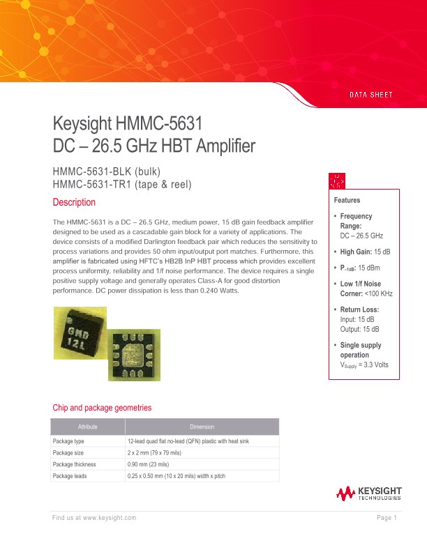
The HMMC-5631 is a DC – 26.5 GHz, medium power, 15 dB gain feedback amplifier designed to be used as a cascadable gain block for a variety of applications. The device consists of a modified Darlington feedback pair which reduces the sensitivity to process variations and provides 50 ohm input/output port matches. Furthermore, this amplifier is fabricated using HFTC’s HB2B InP HBT process which provides excellent process uniformity, reliability and 1/f noise performance. The device requires a single positive supply voltage and generally operates Class-A for good distortion performance. DC power dissipation is less than 0.240 Watts.
Absolute Maximum Ratings [1]
Symbol |
Parameters / Conditions |
Min. |
Max. |
Units |
Vcc |
Collector Pad Voltage |
|
4 |
volts |
Iout |
Maximum Collector Current |
|
50 |
mA |
Pin |
CW Input Power |
|
10 |
dBm |
Tj |
Maximum Junction Temperature [2] |
|
150 |
°C |
TA [2] |
Ambient Temperature |
-55 |
75 |
°C |
Tstg |
Storage Temperature |
-65 |
165 |
°C |
Tmax [3] |
Maximum Assembly Temperature |
|
260 |
°C |
DC specifications / physical properties [1]
Symbol |
Parameters / conditions |
Min. |
Typ. |
Max. |
Units |
Vout |
Output pad voltage |
2.6 |
2.9 |
3.3 |
Volts |
Vin |
Input pad voltage |
1.4 |
1.7 |
2.0 |
Volts |
Ic1 |
Stage one supply current |
28 |
32 |
36 |
mA |
Ic2 |
Stage two supply current |
|
40 |
|
mA |
RF specifications [1]
Symbol |
Parameters / conditions |
0 - 20 GHz |
|
20 - 26.5 GHz |
|
Units |
|||
|
|
Min. |
Typ. |
Max. |
Min. |
|
Typ. |
Max. |
|
BW |
Operating Bandwidth |
|
20.0 |
|
|
|
26.5 |
|
GHz |
S21 |
Small Signal Gain |
14 |
15.5 |
18 |
12 |
|
14.5 |
18 |
dB |
RLin |
Input Return Loss |
5 |
15 |
|
4 |
|
6 |
|
GHz |
RLout |
Output Return Loss |
5 |
15 |
|
4 |
|
6 |
|
dB |
ISO |
Reverse Isolation |
|
-19 |
-15 |
|
|
-20 |
-15 |
dB |
P-1dB |
Output Power at 1dB Compression |
|
15 |
|
|
|
13.5 |
|
dBm |
NF |
Noise Figure |
|
5.5 |
|
|
|
6 |
|
dB |
Biasing
The HMMC-5631 can be operated from a single positive supply. This supply must be connect-ed to two pins on the IC, namely the VCC pin and the OUT pin. The supply voltage may be directly connected to the VCC pin as long as the voltage is between +3.0 to +4.0 Volts. However, if the supply is higher than +4 Volts, a series resistor (RCC) should be used to reduce the voltage to the VCC pad. See the biasing diagram below for the equation used to set RCC. In the case of the OUT pin, the supply voltage must be connected to the output transmission line through a resistor (ROUT) and an inductor. See the biasing diagram for the equation used to set ROUT. If ROUT is greater than 300 ohms, the inductor may be omitted; however, the amplifiers gain may be reduced by ~0.5 dB.
The voltage at the In and OUT pins of the IC will be approximately 1.7 and 2.9 Volts respectfully; therefore, DC blocking caps should be used at the input and output of the device.
Assembly Techniques
The HMMC-5631 is fabricated using an InP-based HBT semiconductor material structure which limits the maximum assembly temperature to 150 C. Due to the fact AuSn solder die-attach temperatures exceed this limit, only epoxy-based die-attach materials and processes (such as 84-1LMI) should be employed during HMMC-5631 assembly.
GaAs and InP MMICs are ESD sensitive. ESD preventive measures must be employed in all aspects of storage, handling, and assembly.
Keysight application note, “GaAs MMIC ESD, Die Attach, and Bonding Guidelines" provides basic information on the subjects.