



Why Choose Keysight Photonics Design Suite
From device innovation to system validation.
As photonic technologies become essential for AI infrastructure, datacenter interconnects, communications, sensing, and quantum applications, engineering teams need design tools that connect device physics with real-world system performance. Keysight Photonics EDA solutions provide an integrated workflow for modeling, designing, analyzing, and optimizing photonic devices, photonic integrated circuits (PICs), optical subsystems, and complete transmission systems. The portfolio enables engineers to move seamlessly from component-level design and verification to circuit and system-level simulation, helping reduce development risk, accelerate innovation, and improve first-pass success. Whether developing foundry-ready PICs, validating optical connectivity, or evaluating end-to-end link performance, Keysight provides scalable tools that support the entire photonic design lifecycle. The combined portfolio delivers comprehensive photonic design automation spanning devices, circuits, and systems.
- Device Simulation
- Component Design
- Transmission Design
- Link Engineering
Photonic Design Software
(RSoft Photonic Design Tools)
Accelerate design for state-of-the-art photonic components and systems with rigorous modeling and simulation software.
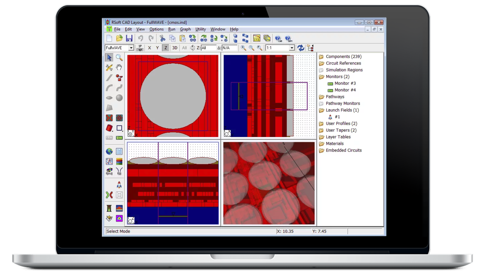
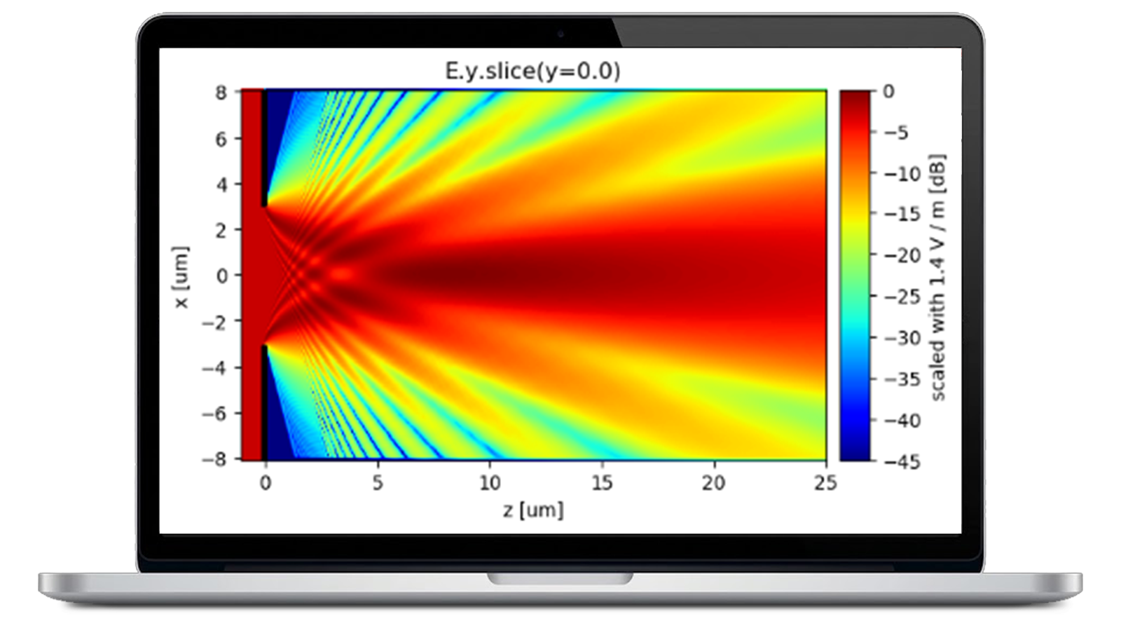
Photonic Device and Fiber Simulation
(VPIdeviceDesigner)
Design, simulate, and optimize photonic devices with confidence.
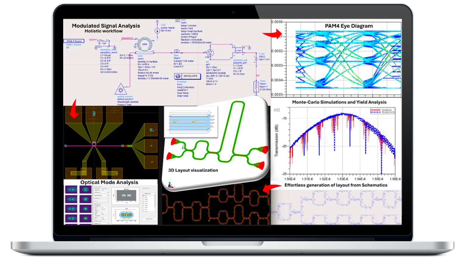
Photonic Designer
Keysight Photonic Designer delivers a comprehensive photonic designer automation (PDA) solution that bridges the gap between innovative concepts and practical implementation.
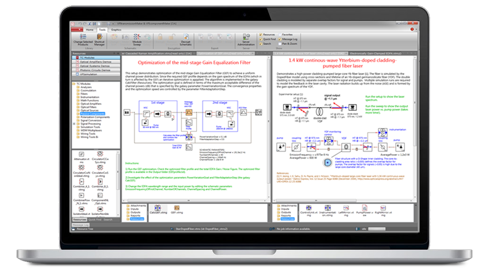
Fiber Amplifier and Laser Simulation
(VPIcomponentMaker Fiber Optics)
Model, optimize, and innovate next-generation fiber optic technologies.
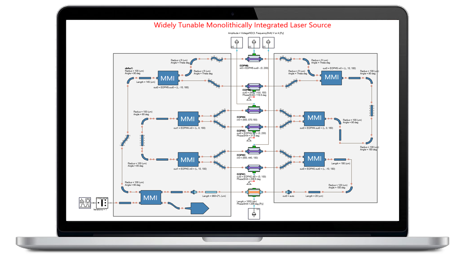
Photonic Integrated Circuit Simulation
(VPIcomponentMaker Photonic Circuits)
Design, simulate, and optimize advanced photonic integrated circuits.
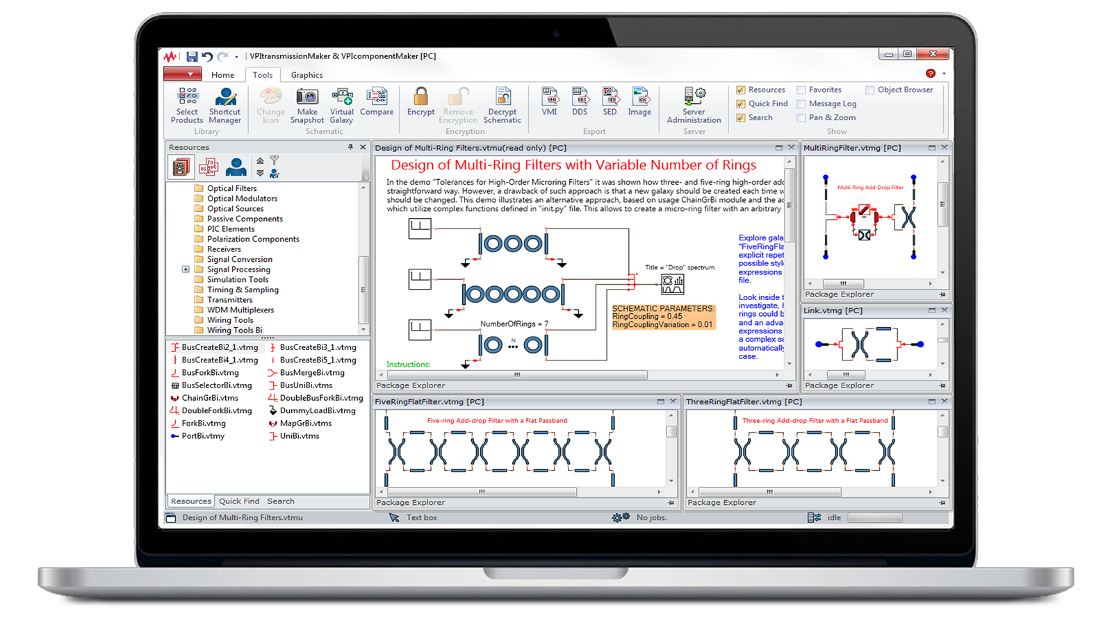
Photonic Foundry PDK Library
(VPItoolkit PDK <fab>)
Accelerate photonic IC development with layout-aware PDK-driven design.
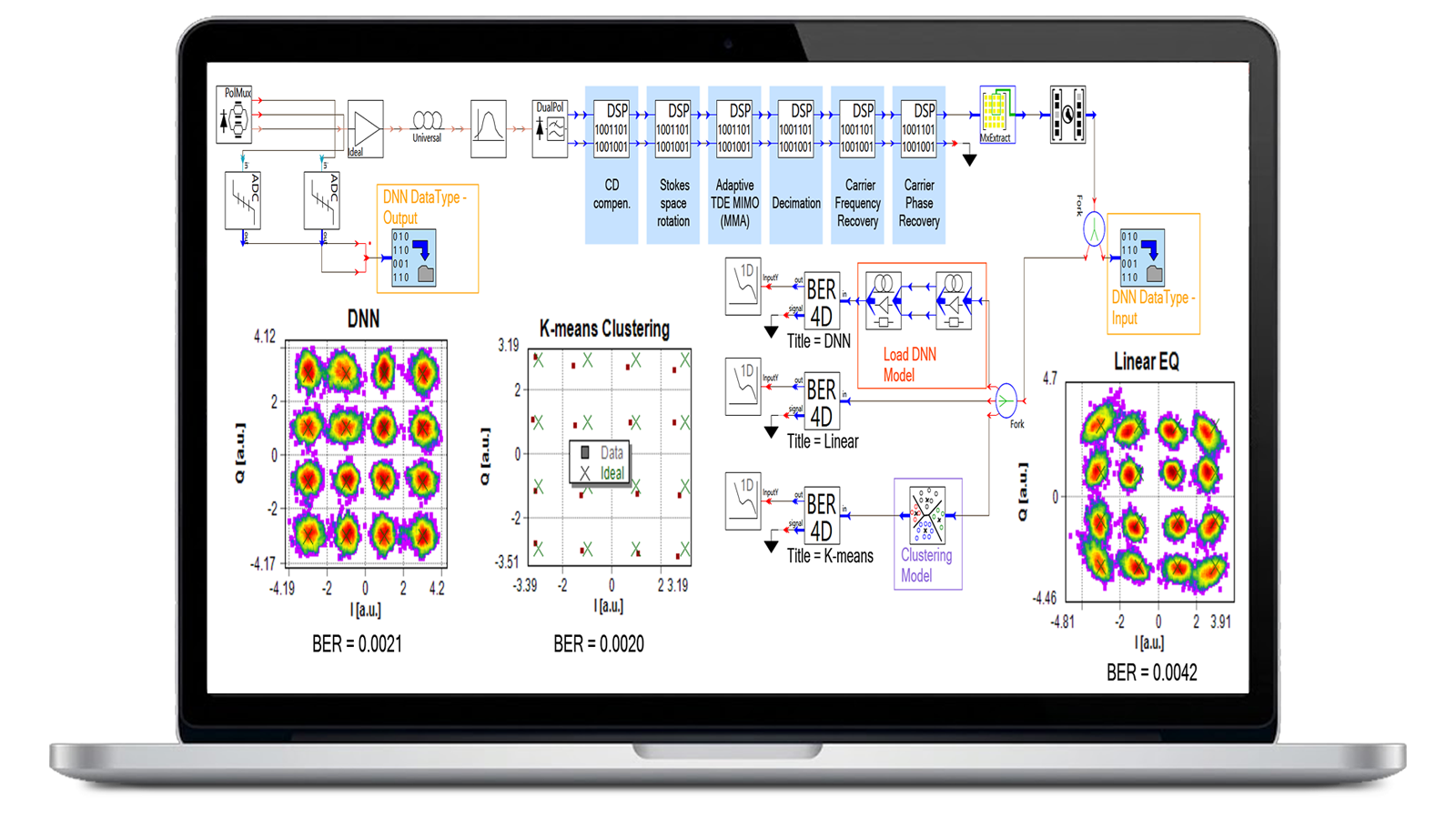
Machine Learning for Photonic Simulation
(VPItoolkit ML Framework)
Accelerate photonic device innovation with advanced electromagnetic simulation.
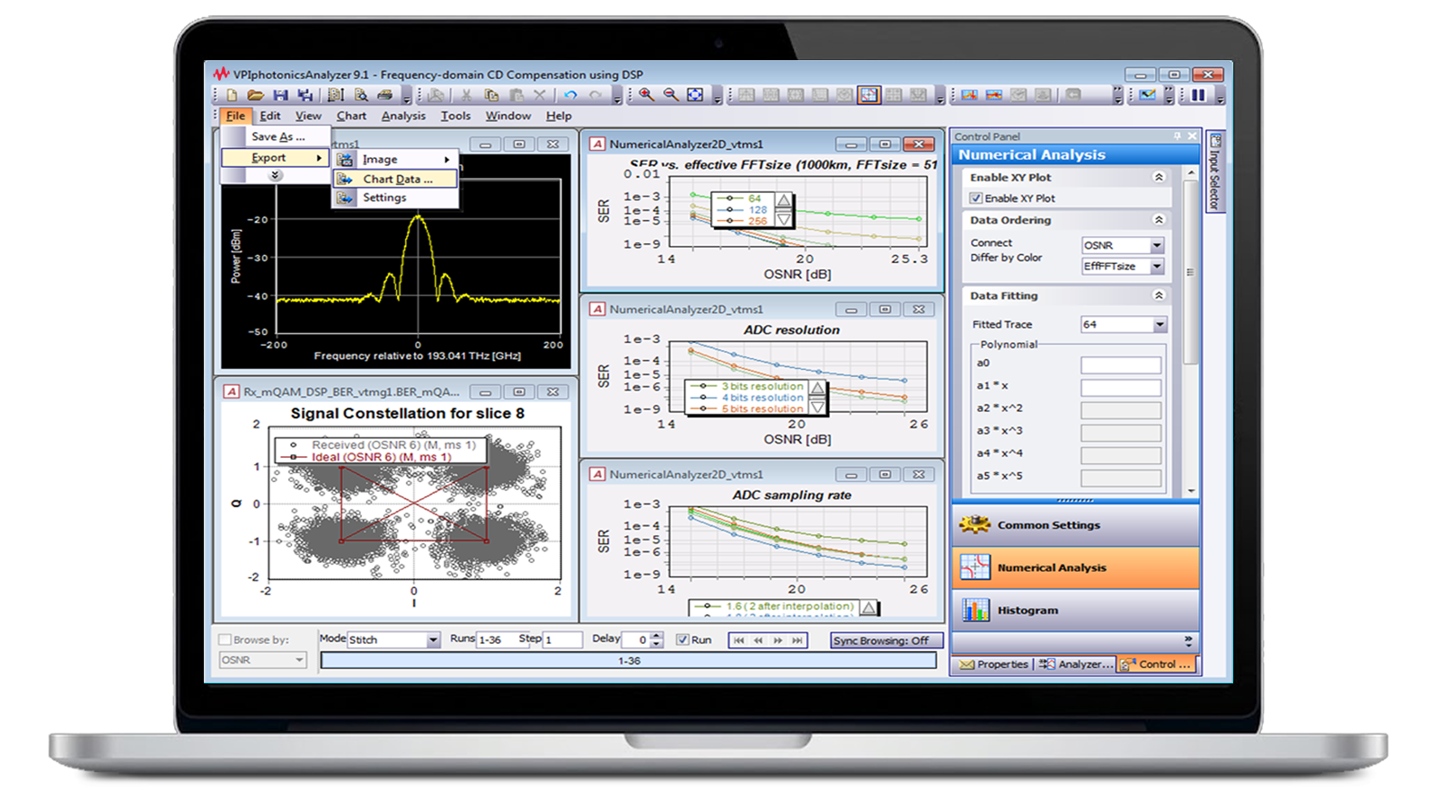
Photonic Simulation Environment
(VPIphotonics Design Suite)
Accelerate photonic IC development with layout-aware PDK-driven design.
Advanced Design System (ADS)
Accelerate your workflow using circuit design and simulation software with integrated guidance and templates.

Optical Transmission System Simulation
(VPItransmissionMaker Optical Systems)
Accelerate the design of new photonic systems and subsystems.
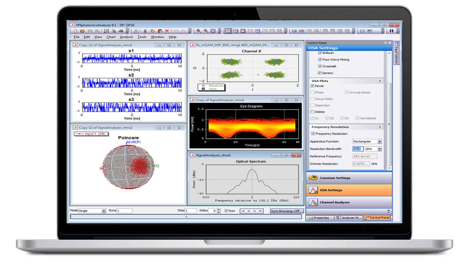
Test Signal Generation and Analysis
(VPIlabExpert)
Bridge simulation and laboratory testing for faster photonic innovation.
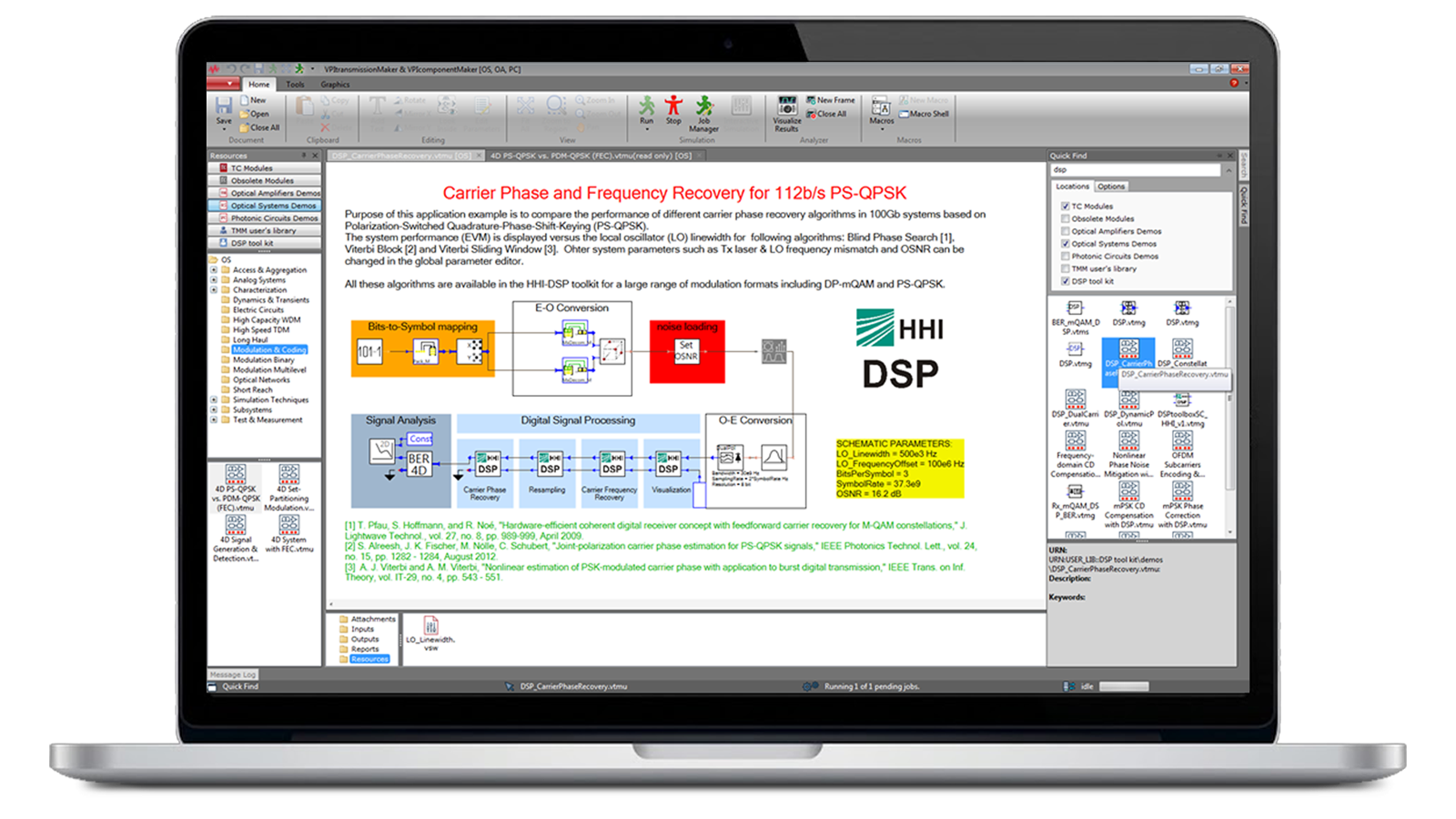
DSP Algorithm Library
(VPItoolkit DSP Library)
Accelerate coherent optical innovation with advanced digital signal processing.
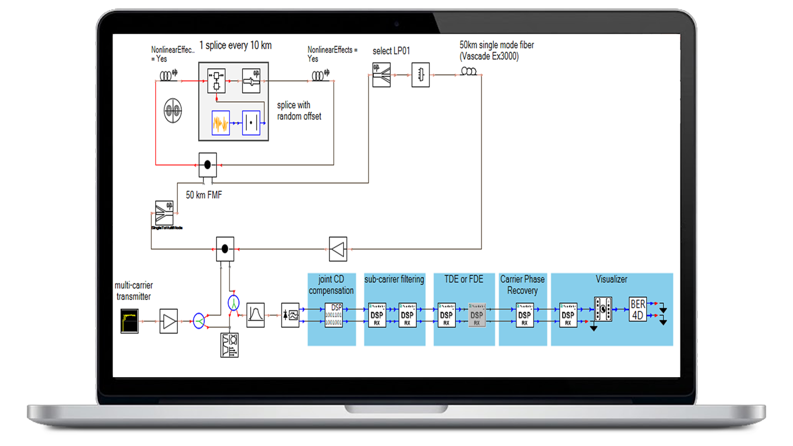
Machine Learning for Photonic Simulation
(VPItoolkit ML Framework)
Accelerate photonic device innovation with advanced electromagnetic simulation.
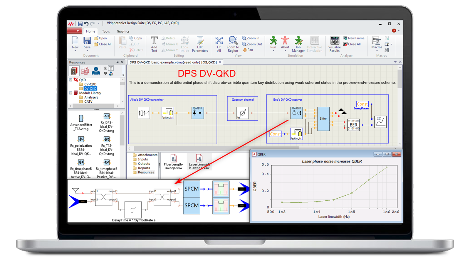
Quantum Key Distribution Simulation
(VPItoolkit QKD)
Model, validate, and optimize secure quantum communication networks.
Photonic Simulation Environment
(VPIphotonics Design Suite)
Accelerate photonic IC development with layout-aware PDK-driven design.
Optical Network Planning
(VPIlinkConfigurator)
Automate optical network planning, optimize performance, and accelerate deployment decisions.
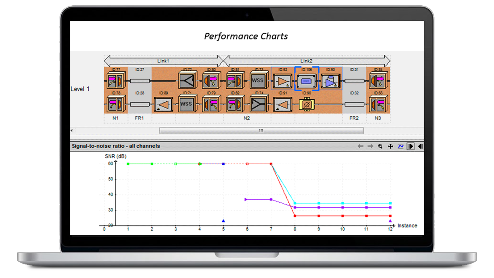
Optical Network Design
(VPIlinkDesigner)
Accelerate optical network design with real-time performance insight.
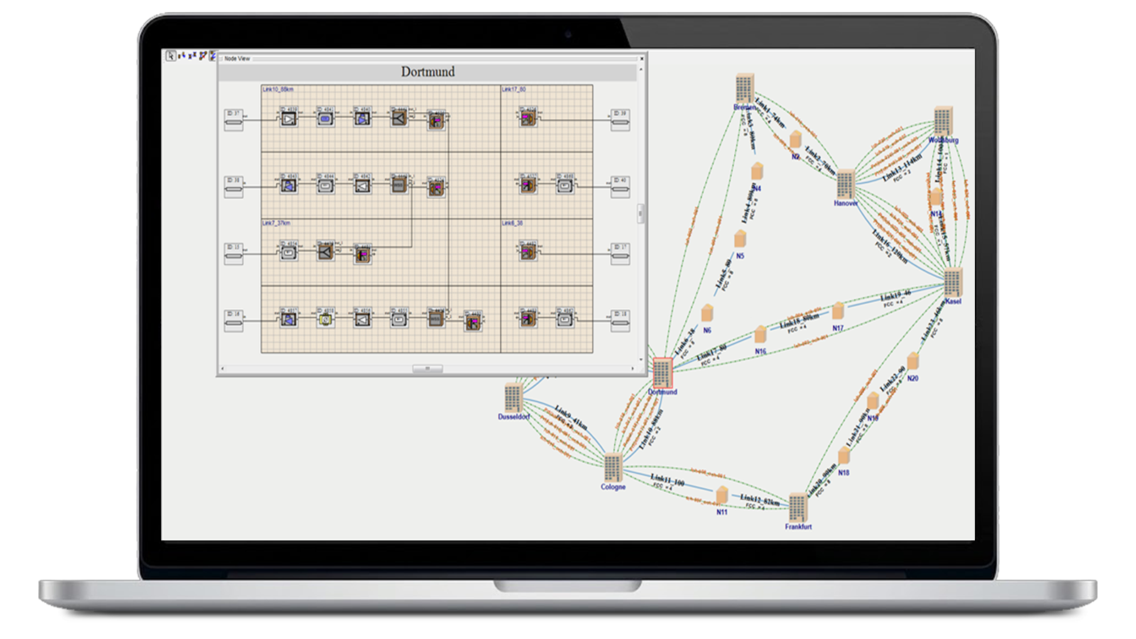
Resources to Get You Started
This brochure presents Keysight’s VPIphotonics portfolio for end-to-end photonic design automation. It covers tools for integrated photonic circuits, optical devices, fiber amplifiers and lasers, transmission systems, and network planning. Key capabilities include interactive simulation, automated optimization, scripting, accelerated computing, and data visualization. Interfaces with third-party software and laboratory equipment support collaborative workflows, while protected model sharing enables design exchange without exposing proprietary information.


Application Notes
Optimizing Photodetector Model to a Silicon Photonics Foundry Process

Application Notes
Design and Simulation of a Mach-Zehnder Modulator with Push-Pull Configuration
Application Notes
Custom PDK Generation for a Ring Resonator
Application Notes
End-to-End Electrical-Optical-Electrical Flow in Keysight ADS
WEBINARS
End-to-End Co-Design for Ethernet: Bridging Photonics and Electronics with EOE Simulation

Brochures
RSoft Photonic Device Tools
Have Questions? We've Got Answers
Photonics EDA (Electronic Design Automation) software enables engineers to design, simulate, optimize, and verify photonic devices, photonic integrated circuits, optical subsystems, and complete communication systems before fabrication and deployment.
The portfolio includes solutions for photonic device simulation, PIC design and verification, and system-level optical simulation, enabling workflows that span from component physics to complete optical links.
Photonic Designer is best suited for photonic integrated circuit design, layout-driven workflows, circuit verification, foundry PDK integration, and PIC implementation. It focuses on creating and validating PIC architectures before manufacturing.
Photonic Simulation Environment is ideal for modeling and optimizing optical systems, subsystems, transmission networks, fiber-optic components, and complex electro-optical interactions where overall system performance is the primary concern.
Photonic Designer focuses on circuit-level PIC implementation and verification, while the Photonic Simulation Environment extends analysis to subsystem and system-level behavior. Together they provide continuous design insight from photonic circuits to complete optical links.
Yes. The solutions support multi-domain modeling that incorporates photonic, electrical, and optoelectronic behavior, helping engineers understand how devices and circuits perform within larger systems.
Common applications include datacenter interconnects, coherent optical communications, silicon photonics, co-packaged optics, fiber sensing, laser communications, telecommunications networks, and advanced PIC-based systems.
Yes. The platform supports PDK-driven development and reusable photonic building blocks, helping teams move efficiently from design concepts to manufacturable PIC implementations.
By enabling virtual prototyping, performance verification, and end-to-end system evaluation before fabrication, engineers can identify issues earlier, reduce prototype iterations, and accelerate time-to-market.
Choose Photonic Designer when your priority is PIC architecture, layout, and verification. Choose Photonic Simulation Environment when your priority is subsystem, transmission, or network performance. Many organizations use both to create a complete photonic development workflow from device to system.