What are you looking for?
Device Modeling and Characterization
Turnkey solutions for device modeling and characterizing CMOS, RF, and III-V devices
From integrated device manufacturers (IDMs) to top foundries, Keysight provides trusted one-stop solutions that measure, extract, and validate the world’s semiconductor devices. With over two decades of expertise, Keysight's end-to-end device modeling and device characterization solutions, coupled with expert support and state-of-the-art labs, have empowered hundreds of customers to accurately and efficiently model CMOS, RF, and wide-bandgap semiconductor devices.
See What's New in Device Modeling and Characterization.
Device Modeling and Device Characterization Solutions
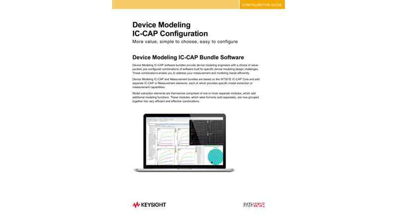
- Device Modeling IC-CAP is versatile, user-programmable industry standard software for DC, analog, and RF semiconductor device characterization and modeling. Today's most advanced semiconductor foundries and IDMs rely on IC-CAP for modeling silicon CMOS, bipolar, compound gallium arsenide (GaAs), gallium nitride (GaN), and many other device technologies.
- Device Modeling MBP provides complete silicon turnkey device modeling software that integrates SPICE modeling and simulation, model parameter extraction, and model library generation.
- Device Modeling MQA is the industry-standard SPICE model validation software, enabling thorough check-model quality and automatic QA and reporting procedures for both silicon and III-V technologies.
- Device Modeling WaferPro supports on-wafer measurement and programming test software for use with a variety of instruments and wafer probes.
- Advanced Low-Frequency Noise Analyzer (A-LFNA) supports on-wafer measurement and analysis of low-frequency noise including flicker noise and random telegraph noise.
Watch the latest Device Modeling product update webinars

Simplifying and Automating Compact Model Process with Machine Learning
See how the Machine Learning Optimizer in Device Modeling MBP dramatically improves modeling efficiency by automating and simplifying complex workflows.

RTN Measurement and Stress-testing using A-LFNA/WaferPro
Learn about the best practices for RTN detection, large data post-processing, remote control, and integration into reliability workflows.

Keysight EDA Solutions for Semiconductor Foundries
The semiconductor industry is at a massive inflection point. On one hand, devices featuring trillions of transistors and wide bandgap semiconductors are making waves across the electronic design industry. The combination of exploding volume of data and more complex models significantly increases pressure to meet time-to-market expectations. On the other hand, regional initiatives such as the CHIPS Act create unprecedented demand and growth opportunities. Foundry leaders will need to focus strategically on modernizing workflows to boost productivity and unlock areas of opportunity. Keysight EDA is at the forefront of this shift, working in close collaboration with foundries to deliver high quality models and PDKs tailored for Si, SiGe, GaAs, InP, and GaN processes. Our software and services form a total solution covering test structure design, device characterization and modeling, PDK creation, validation, and process and data management. Partner with Keysight EDA to innovate faster and smarter beyond Moore’s Law.
Accelerating Semiconductor Innovation through Machine Learning-Driven Device Modeling
Traditional modeling approaches are increasingly challenged by the complexity, scale, and speed required in modern design environments. From neural network-based models that eliminate the need for manual parameter tuning to hybrid neural network architectures that blend physical insight with data-driven adaptability and ML-powered modeling workflows, these technologies enable faster, more accurate, and more scalable modeling solutions.
The applications and benchmarks presented demonstrate that AI/ML-based modeling not only improves predictive accuracy across DC, RF, and large-signal regimes but also reduces development time, enhances generalization across device variants, and lowers the barrier to entry for model developers.

Protect Your Innovation Investment
Featured Resources
Frequently Asked Questions
Device modeling refers to the process of creating mathematical and physical models to predict the behavior of semiconductor devices, such as transistors, diodes, and capacitors. These models help electronic designers understand how these components perform in various real-world applications.
Device modeling enables design engineers to optimize their designs for specific requirements, such as maximizing speed or minimizing power consumption. By simulating device behavior under different conditions, engineers can effectively reduce the need for expensive physical prototypes, thereby saving time and resources.
The typical flow of device modeling and characterization consists of four critical steps, with each integral to the quality and reliability of the final models:
- Data measurement and analysis: This first stage involves gathering measured data from various semiconductor devices across different wafers and temperatures. The focus here is on precision and efficiency.
- Model extraction: Model extraction complexity varies with the technology and specific device model. Device modeling software is instrumental at this stage, offering advanced graphics, links to circuit simulators, optimizers, and manual tuners to extract parameters. For RF modeling, custom programming might be necessary to account for parasitic effects in S-parameters.
- Model validation: This step is fundamental to ensure the reliability of the modeling libraries by running simulations over extended bias, geometry, and frequency conditions. Tools like Device Modeling MQA (Model Quality Assurance) can automate much of this process, simplifying the testing and helping to identify and report any issues efficiently.
- Integration into process design kits (PDKs): The final step involves integrating device modeling libraries into PDKs. A critical but challenging aspect of this phase is PDK validation, which involves extensive re-verification of sample designs whenever there's a new release of a simulator software version or an update to a design kit. The goal is to ensure that the PDKs remain accurate and consistent across different updates.
Want help or have questions?


