
P9001A Massively Parallel Parametric Test System
Brochures
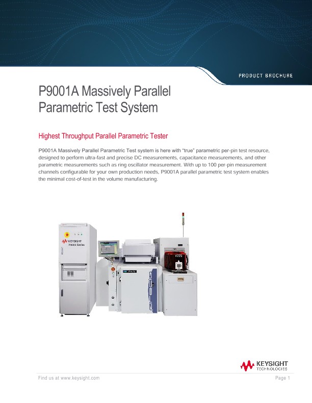
The current web page context is a PDF document that introduces the P9001A Massively Parallel Parametric Test System, a product from Keysight Technologies that offers the highest throughput parallel parametric testing for semiconductor wafer production. The document provides detailed information on the hardware, software, and professional services that are included in the total solution of the P9001A test system.
The P9001A test system has up to 100 per-pin measurement channels that can perform ultra-fast and precise DC measurements, capacitance measurements, and other parametric measurements such as ring oscillator measurement. The system also has shared test resources such as a digital voltmeter and an LCR meter for enhanced measurement capabilities. The system can be configured and upgraded according to the customer's production needs and test structure design.
The P9001A test system uses Keysight SPECS (Semiconductor Process Evaluation Core Software) and the SPECS Parallel Test Extension software to perform massively parallel test with synchronous or asynchronous parallel mode. The software allows the user to define parallel test flexibly and scalably with intuitive interfaces and algorithms. The software also supports factory automation with SPECS-FA (Factory Automation) version. The software comes with a 36-month subscription service that includes software license-to-use, software media, and remote technical support.
Keysight also offers various professional services to complete the parametric tester solution, such as on-site installation, warranty and extended services, calibration services, productivity assistance, application software support, startup assistance, training, post-sales service, and contract renewal. These services are provided by Keysight experts who have deep domain knowledge of test equipment, software, standards, and regulations.
The P9001A Massively Parallel Parametric Test System is designed to help customers overcome typical but difficult process test challenges in semiconductor wafer production, such as improving throughput, minimizing downtime, reducing cost of test, and maximizing productivity and production capacity. Customers can contact their local Keysight office or visit www.keysight.com/find/contactus for more information on the product, applications, or services. Customers can also learn more about the product at www.keysight.com/find/P9001A.