What are you looking for?
HeatWave Case Studies
The two case studies below describe how HeatWave electro-thermal analysis software was used to solve challenging design issues with a signal amplifier IC design and a mobile transceiver chip design..
Data Channel Amp
A mixed-signal design team at a large IDM redesigned a signal amplifier IC for an electromechanical device. The designers retargeted the chip to run faster on a smaller process node. The new chip was no longer housed in a package; instead, the bare die was solder bumped and attached directly to the device in a mobile form factor. Because the previous version had been in production for some time, minimal changes were made to the functional design of the new version, and the team was confident that the redesign would go smoothly.
Worst Case Scenario: Field Failure
However, after the product was deployed, consumers reported field failures. Once the design team isolated the failure to the bare-die amplifier IC, they began emergency debug procedures.
The failure was isolated to a data channel that exceeded the maximum temperature specs. However, the design team was unable to reproduce this failure in the lab. The operational modes of the bare-die chip were the same as the packaged chip, which worked fine in high volume production. What was causing the bare-die version to fail?
The team suspected that the problem was related to temperature, so they retained the Virtual Thermography team to perform thermal simulations using HeatWave on the new amplifier IC. Together, the Virtual Thermography team and the design team gathered the required layout, thermal model, and die material data in order to run the thermal simulation.
Pinpointing the Failure Mode
The HeatWave electro-thermal simulation pinpointed the failure mode within hours. On sustained data transfer through a single amplifier channel, a group of matched transistors were subjected to a ΔT of over 7°C. This caused the amplifier bias currents to be mismatched, which caused the signal path to malfunction. The new circuit simulation, with device temperatures annotated, confirmed the malfunctioning behavior.
The ΔT in one matched group among many matched groups is easily overlooked. The designers did not anticipate that a sustained burst on one channel would result in such a high ΔT on this particular group of matched transistors. This failure mode was also masked in the prototype testing because the die was attached to a heat spreader bar in a package, resulting in a much smaller ΔT across the matched transistors.
The team realized that if they had performed the thermal simulation before fabricating the bare-die version, they would have caught the problem and prevented the expensive field failure.
Mobile Transceiver
A mobile transceiver chip was designed by a fabless IC company and built on a SiGe BiCMOS process. The chip functioned properly in most aspects, except that it fell short of the RF power output specification. So the analog and RF design team rushed to debug and correct the problem.
Silicon Does Not Meet Spec
The chip was specified to produce 24dBm output power at 1.9GHz. However, the first silicon data showed the power output was half, or 3dB less than the target. Detailed analysis of silicon data versus simulation showed the RF power amp was weaker than expected. The power transistors dissipate heat in a concentrated area, which can cause significant temperature peaks and variations. The HeatWave Virtual Thermography team was called to perform thermal simulations using HeatWave. Together, the HeatWave Virtual Thermography team and the design team gathered the required layout, thermal model, and die material data as input for the thermal simulation.
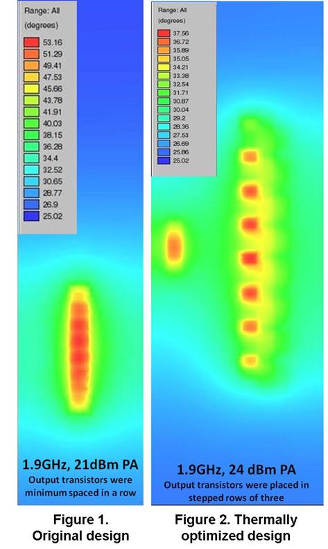
In the original design, the transistor segments were placed in a straight line with minimum spacing. Thermal simulation showed a temperature variation (ΔT) exceeding 28°C within the chip, and 12°C within the power transistor (see Figure 1.). This temperature data was annotated back into the circuit simulation, showing 21dBm output power at 1.9GHz, and matching the degraded silicon performance. This confirmed that the RF power amp efficiency was degraded by the temperature variations across the transistor segments.
Eliminating the Thermal Blind Spot
In order to reclaim the power amp efficiency, the designer experimented with several different transistor segment placements, within the constraints of the existing chip layout. A version with the transistor segments placed in a diagonally staggered pattern was chosen, because the thermal simulation showed a much improved ΔT of 12°C within the chip and only 5°C within the power transistor segments (see Figure 2.), while minimizing the disruption to the rest of the chip layout.
Within a turnaround time of 2-3 hours, thermal simulation provided the designer with a fine-grain temperature profile of the full chip, enabling him to quickly identify a layout topology that minimized the temperature variations across the power transistors. Circuit simulation using the correct device temperatures confirmed that the new design would meet the target spec of 24dBm at 1.9GHz. This was later verified by lab measurement.
Because this chip has areas of high power density, the original circuit simulations, which assumed uniform temperature for the entire chip, produced misleading results. Precise device temperatures, computed using layout and power at the length scales of the devices, were required in order for the circuit simulation to provide relevant results.
Learn more about PathWave Thermal Design (HeatWave) Electro-Thermal Analysis Software.