


Why Choose Keysight High Speed Digital Suite
Design high-speed digital systems with greater confidence.
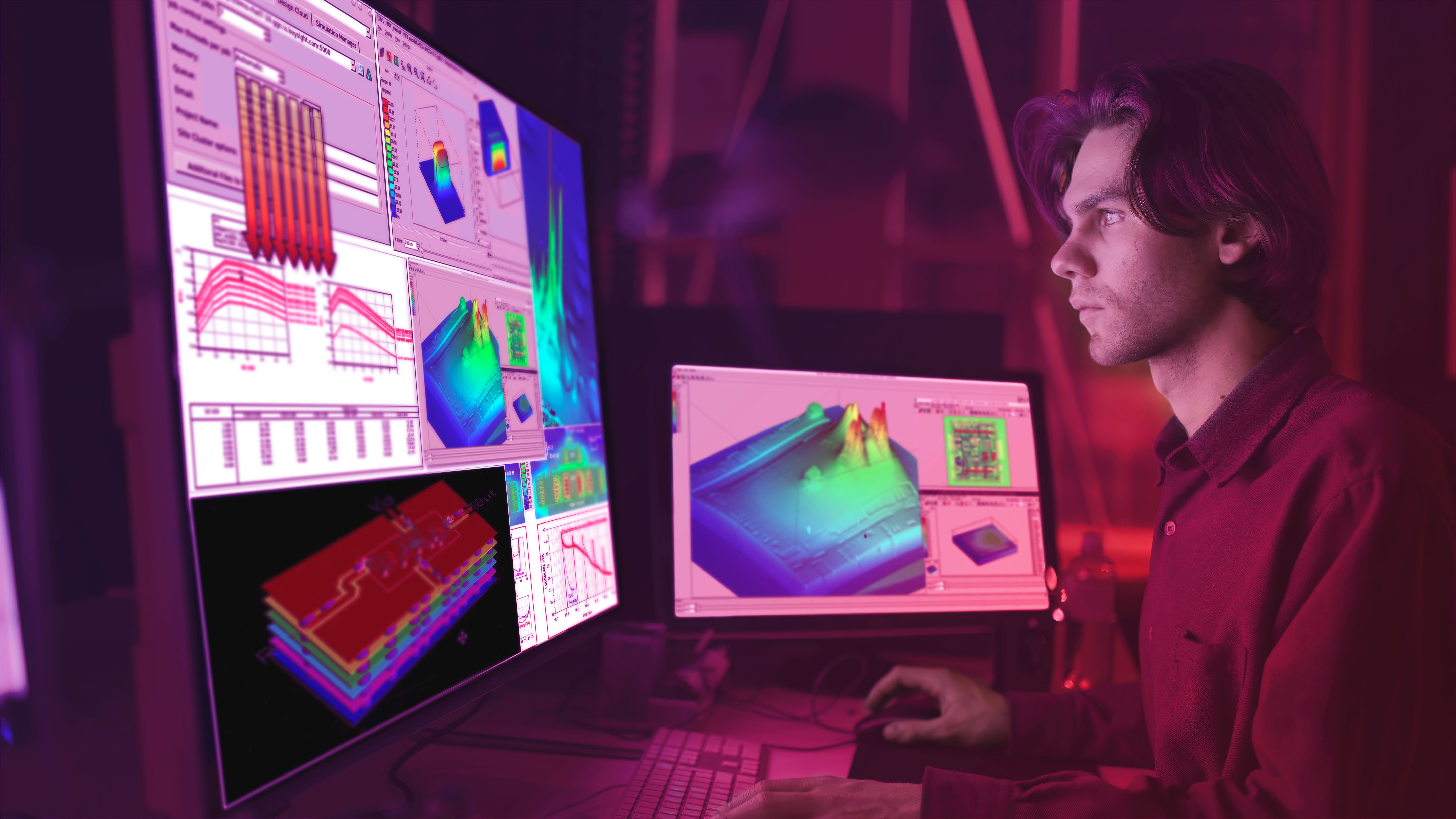
As data rates increase and package complexity grows, engineers need accurate insight across signal integrity, power integrity, compliance, and advanced packaging workflows. Keysight EDA provides an integrated design environment that helps teams analyze complete high-speed digital systems, predict performance before hardware buildout, and validate compliance earlier in the design cycle. The platform enables simulation-driven design decisions for chiplets, advanced packages, PCBs, memory interfaces, and high-speed serial links while reducing development risk, shortening design iterations, and improving first-pass success. Proven through real-world customer applications, Keysight EDA helps engineering teams deliver reliable, compliant, and high-performance products faster.
Advanced Design System (ADS)
EDA platform for High Speed Digital Suite.
Keysight ADS is the premier electronic design automation (EDA) platform for the design of physical layer components that enables engineers to design, analyze, and optimize the critical components that power today's most advanced commercial and defense systems. The base platform contains powerful 3D physical layout and verification, data display, optimization, statistical analysis, Python scripting automation, and AI-Assisted design tools. High-Performance Computing (HPC) options can significantly accelerate simulation times. Additional simulation capabilities such as nonlinear circuit, electromagnetic (EM), electrothermal (ETH) and system provide engineering teams with a choice of value-packed, preconfigured combinations of software modules built for specific design workflows: RF/Microwave, High-speed Digital, Power Electronics, Photonic, and Quantum.


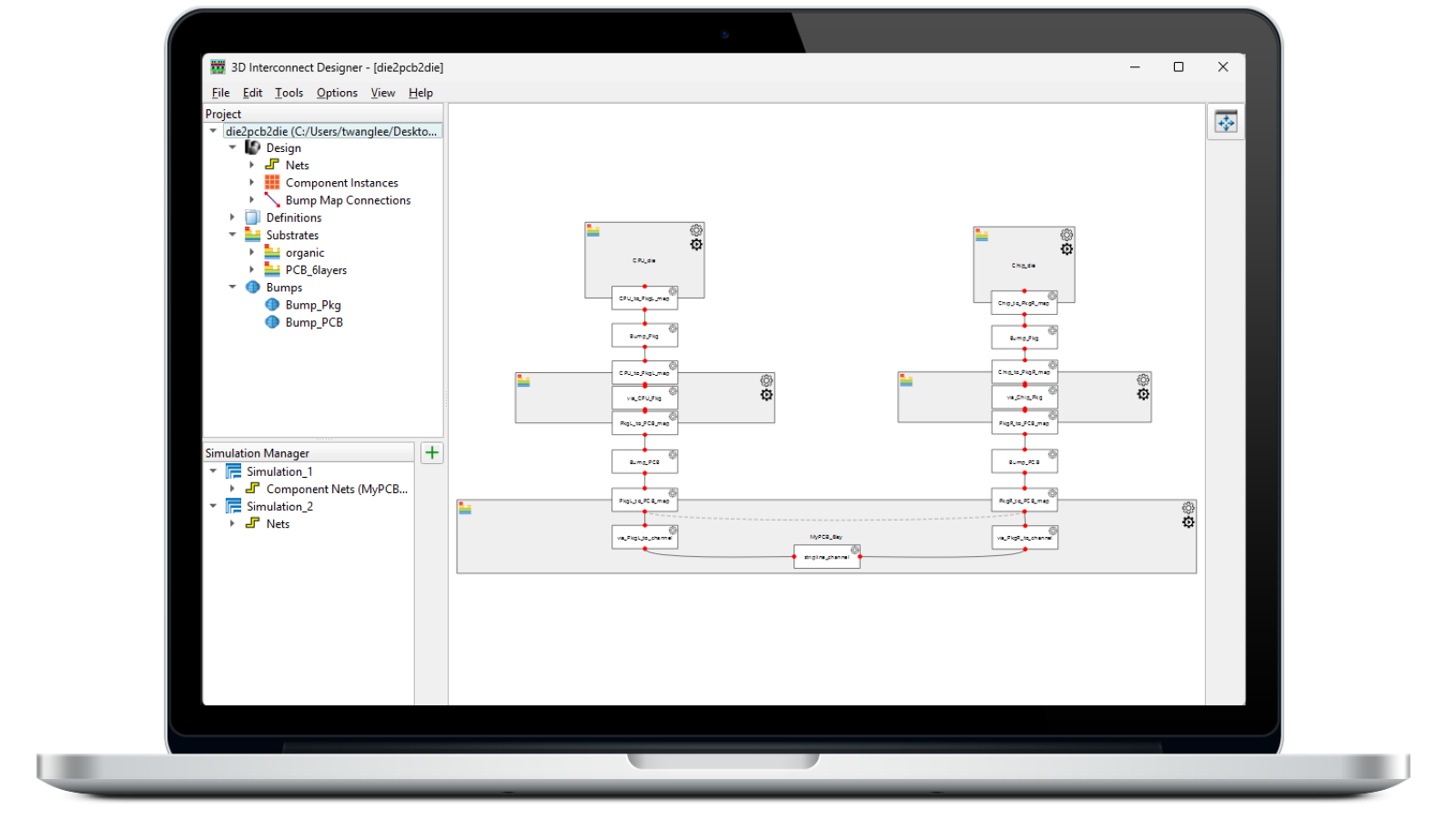
3D Interconnect Designer
Enables engineers to create detailed models of interposers, microbumps, vias, and multi-die interconnect structures for early system validation and performance optimization.
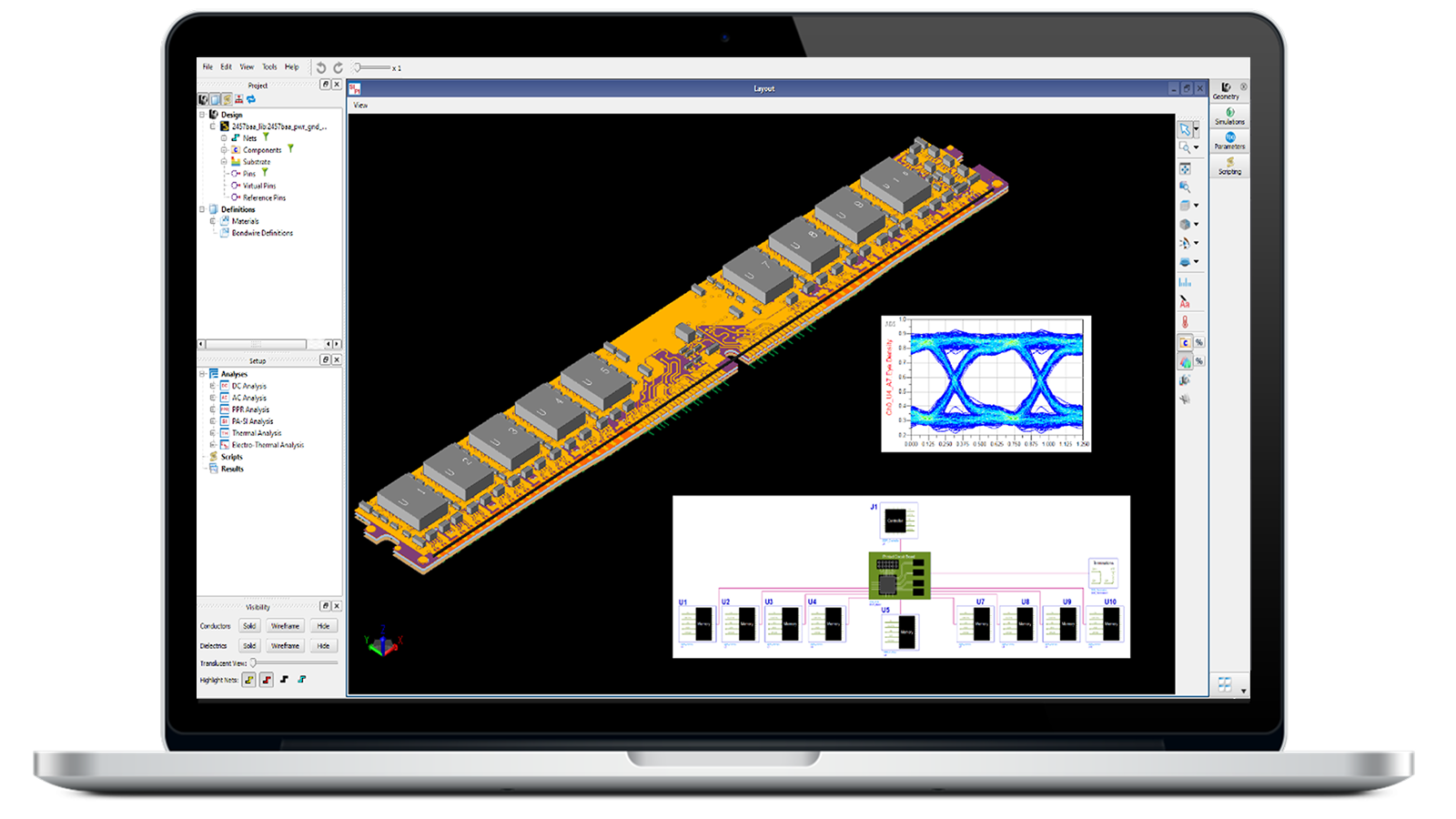
Memory Designer
Shortens design cycles and reduces project delays with the easy-to-use smart components and bus-wires. Also includes compliance testing and DDR bus simulator.
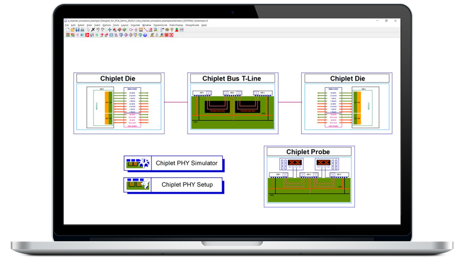
Chiplet PHY Designer
Helps chiplet designers to model and analyze chiplets from D2D PHY to D2D PHY at a system level (D2D: Die to Die PHY) using a smart design environment.
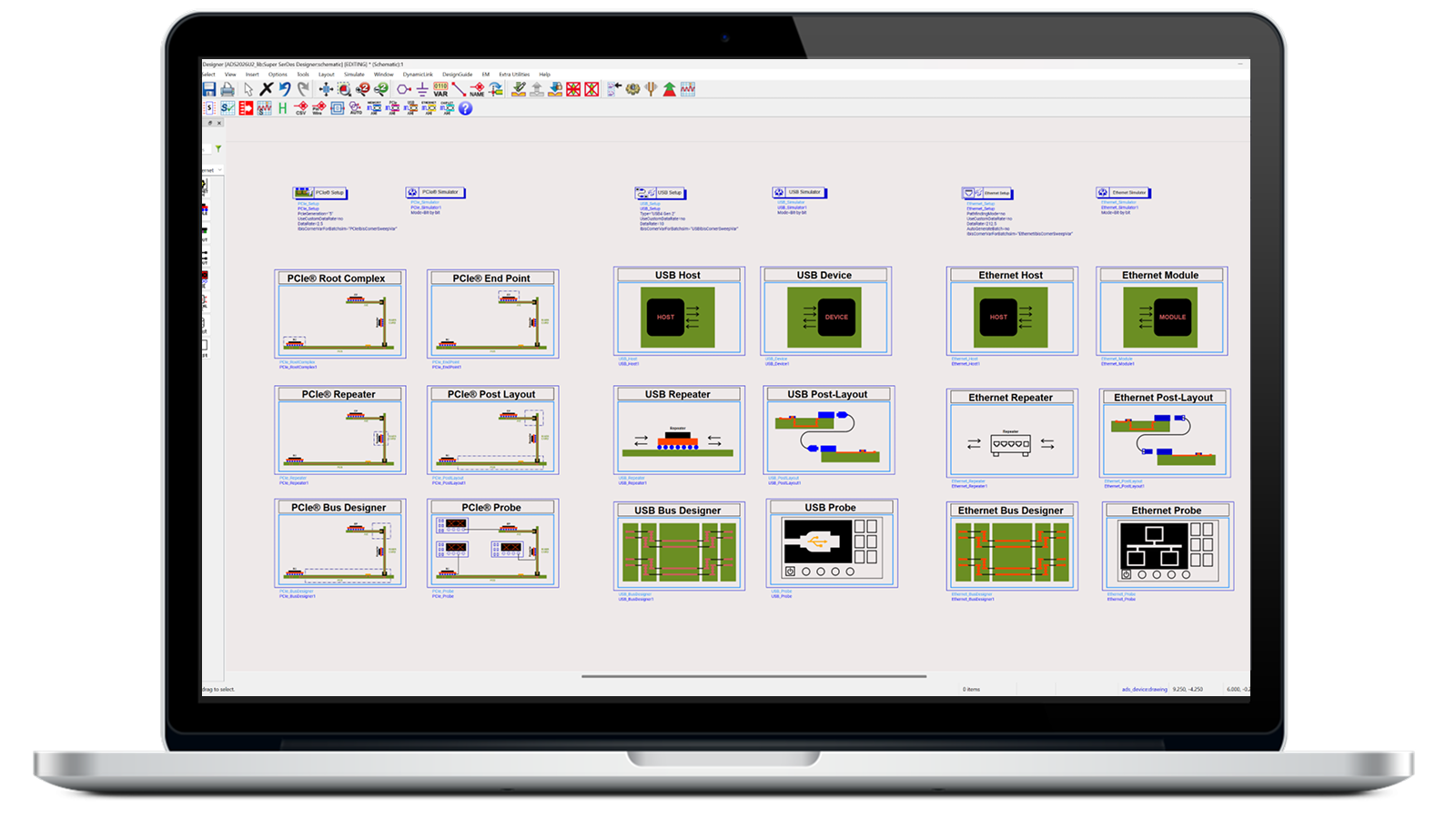
SerDes Designer Bundle
Integrates System Designer for PCIe®, USB, and Ethernet into a single environment, enabling a unified and efficient workflow across multiple SerDes applications.
Chiplet 3D Interconnect Designer
Helps chiplet designers to model and analyze chiplets from D2D PHY to D2D PHY at a system level (D2D: Die to Die PHY) using a smart design environment.
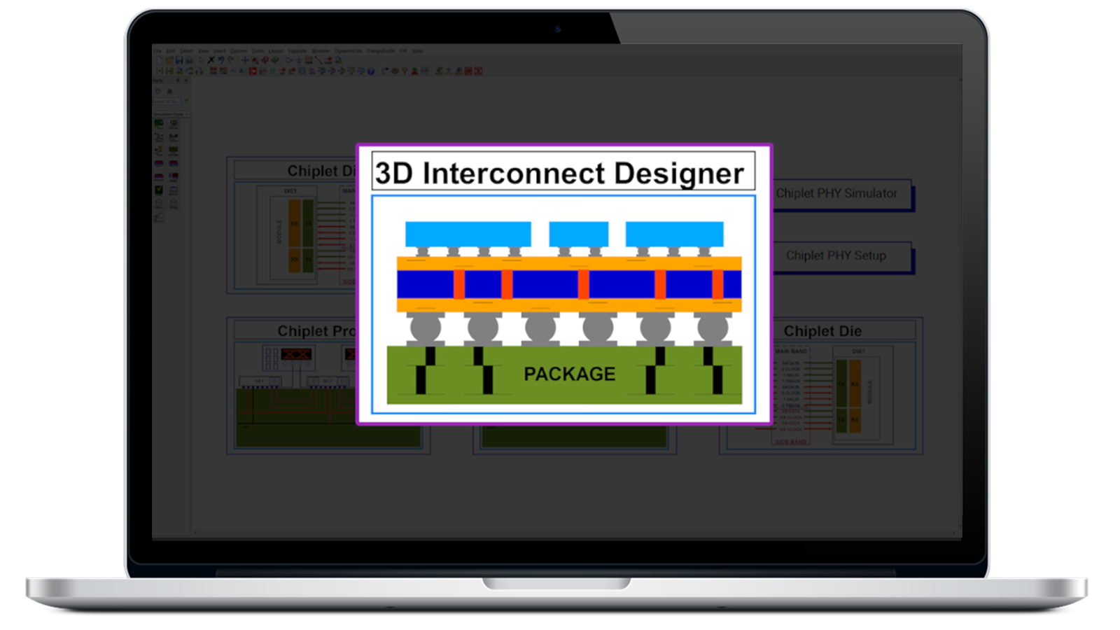
Signal Integrity EM Professional (SIPro)
Provides signal integrity analysis of complex high-speed PCBs, enabling you to characterize signal loss and coupling, and extract an accurate EM model.
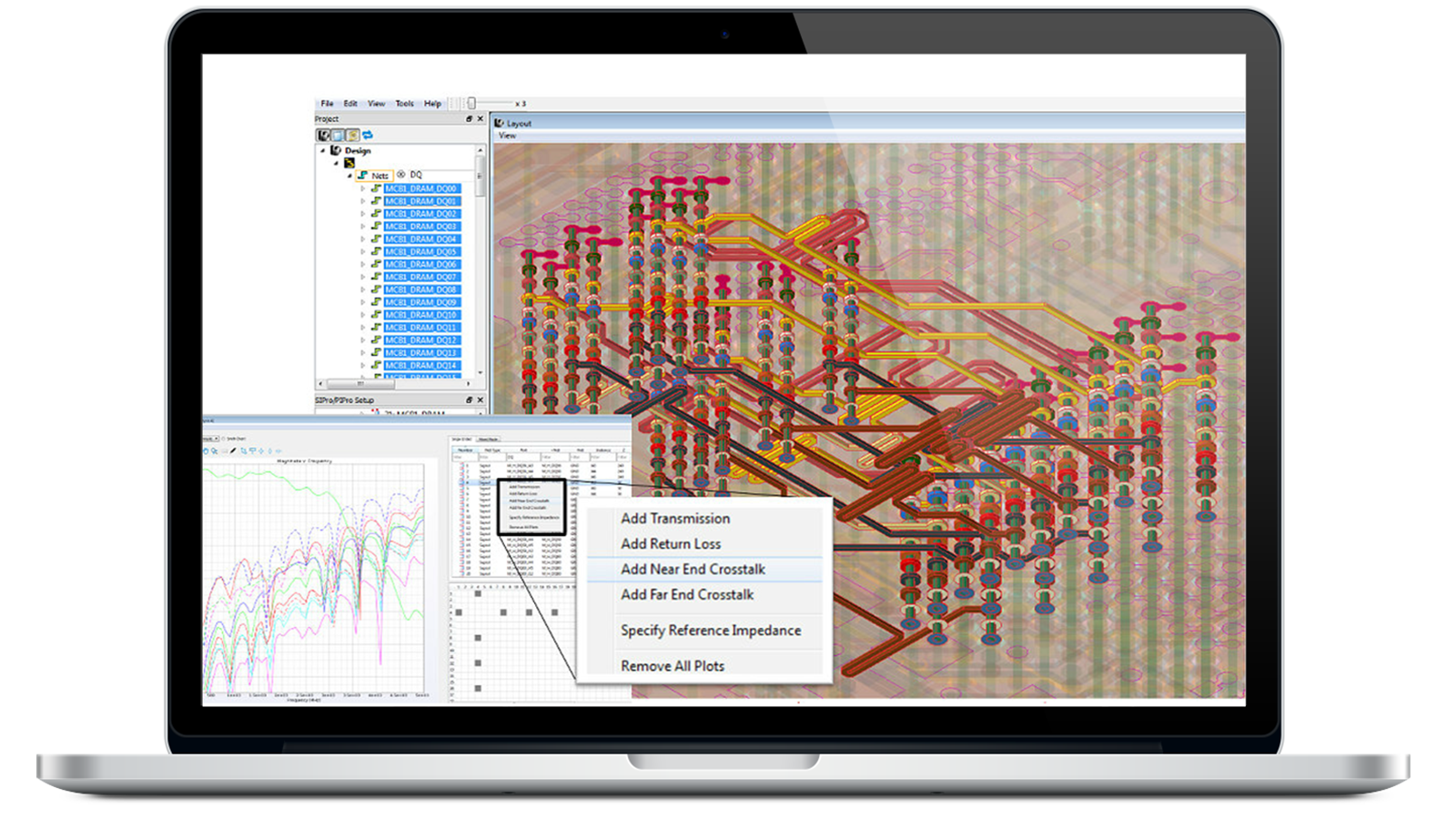
Power Integrity EM Professional (PIPro)
Provides complete power integrity (PI) analysis of your power distribution network (PDN).
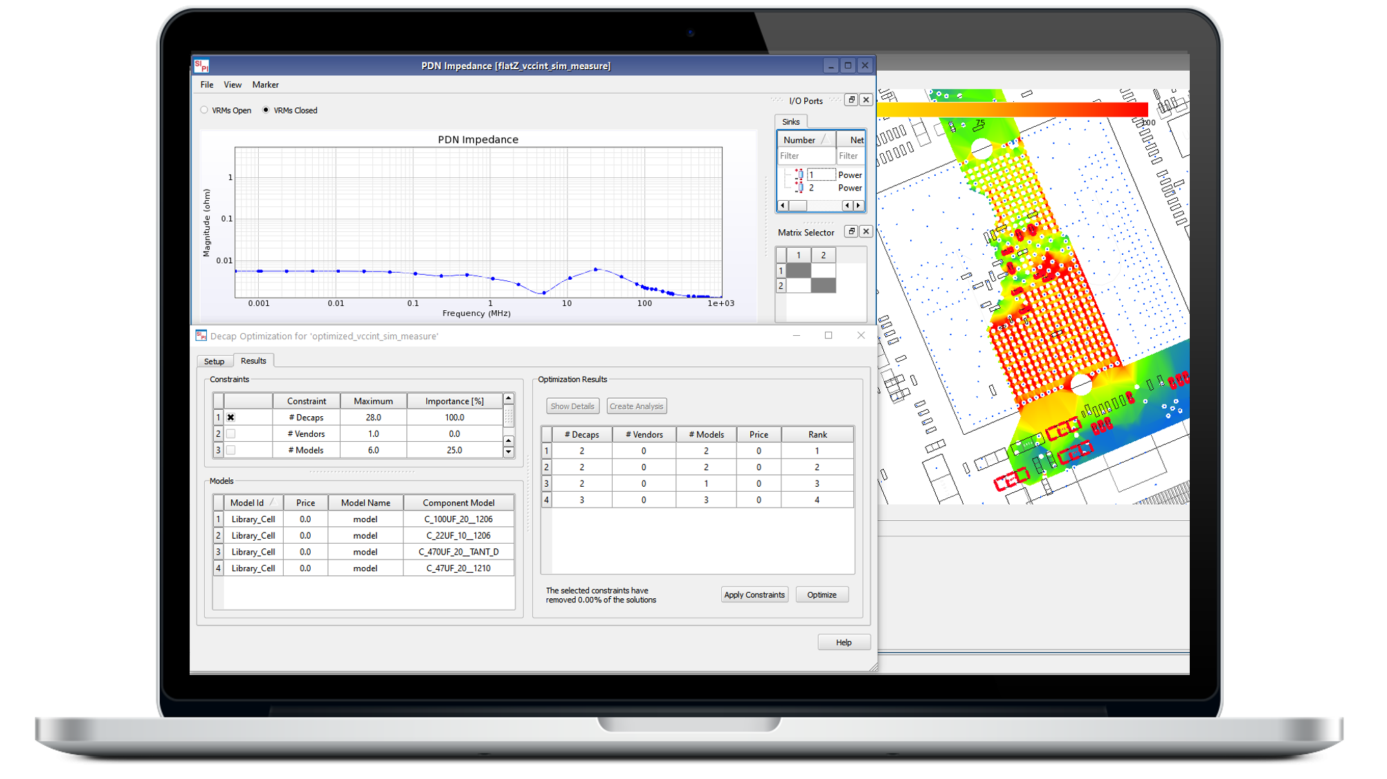
Power Electronics EM Professional (PEPro)
Built for power converter design for power generation and transmission, aerospace-defense, automotive, data center, consumer electronics, and IoT applications.
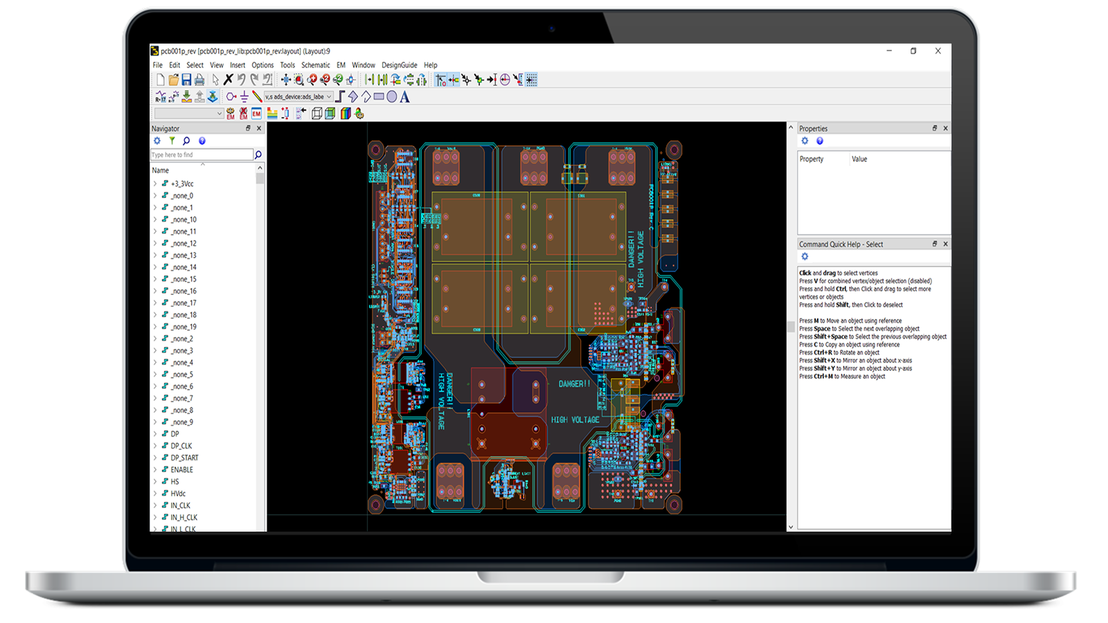


Design Cloud (HPC)
Complex product designs need massive and time-consuming simulations. Keysight Design Cloud leverages High-Performance Computing (HPC) technologies that let you run parallel simulations in the cloud, cluster, or server to reduce simulation time and expedite time-to-market significantly.
Resources to Get You Started
In this webinar, we highlight real-world, customer-driven stories that showcase Keysight EDA’s latest innovations in high-speed digital design. Discover how engineering teams are addressing rapidly evolving standards, mitigating dynamic power integrity challenges, navigating complex hatched ground structures in advanced packaging, and closing the gap between simulation and measurement, all while accelerating design cycles, reducing costly iterations, and moving to product validation with greater confidence.


Explore EDA Bootcamps for e-learning on specific design topics, including high speed digital. Combining webinars, videos, application notes, case studies and blogs, this is a bookmark that you will want to share.

Have Questions? We've Got Answers
Keysight EDA supports high-speed digital applications including data centers, AI infrastructure, memory systems, advanced packaging, chiplet-based designs, and high-speed serial communication links.
The software enables engineers to evaluate signal integrity, power integrity, and compliance performance before hardware fabrication, helping identify issues earlier and reducing costly redesign cycles.
Yes. Keysight EDA provides modeling, simulation, and optimization capabilities for chiplets, stacked die, packages, PCBs, and complex interconnect structures used in advanced packaging technologies.
The solutions are designed for signal integrity engineers, power integrity engineers, system architects, compliance specialists, and design teams developing next-generation digital systems.
Simulation-driven workflows allow teams to predict performance, optimize designs, and verify compliance earlier in the design process, reducing prototype iterations, and accelerating time to market.